Step 2: Building circuits
Result
We assemble a circuit using existing components, visualize the layout and perform a circuit simulation of the entire circuit.
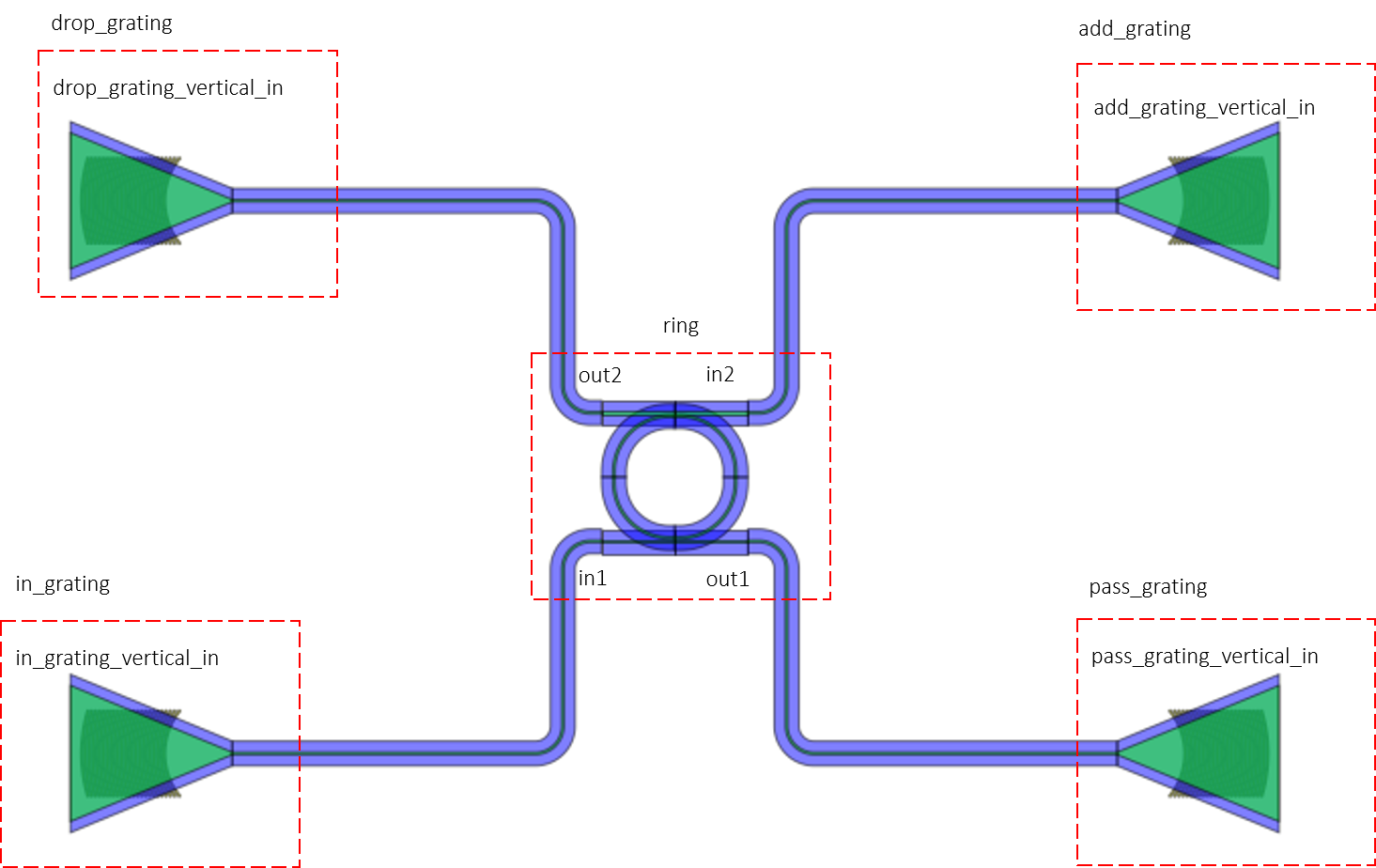
Circuit of a ring resonator coupled to a grating coupler.
Illustrates
how to build a circuit using place and route.
how to perform a circuit simulation of a circuit.
How to run this example
To run the example, run execute_02_circuit.py.
Making the building blocks
The first step is to instantiate the building blocks we will use. As shown in step-1 of this tutorial we instantiate a ring drop filter and a grating coupler.
# 1.  Importing the technology file.
from technologies import silicon_photonics
from ipkiss3 import all as i3

# 2. Import other python libraries.
import numpy as np
import pylab as plt

# 3. Creating the ring resonator
from picazzo3.filters.ring import RingRect180DropFilter
my_ring = RingRect180DropFilter()
my_ring_layout = my_ring.Layout(bend_radius=10.0)

cp = dict(cross_coupling1=1j*0.3**0.5,
          straight_coupling1=0.7**0.5) #The coupling from bus to ring and back


my_ring_cm = my_ring.CircuitModel(ring_length=2 * np.pi * my_ring_layout.bend_radius, # we can manually specify the ring length, or take it from the layout
                                  coupler_parameters=[cp, cp]) # 2 couplers

# 4. Creating the grating coupler.
from picazzo3.fibcoup.curved import FiberCouplerCurvedGrating
my_grating = FiberCouplerCurvedGrating()
my_grating_layout = my_grating.Layout(n_o_lines=24, period_x=0.65, box_width=15.5)
my_grating_cm = my_grating.CircuitModel(center_wavelength=1.55,
                                        bandwidth_3dB=0.06,
                                        peak_transmission=0.60**0.5,
                                        reflection=0.05**0.5)
Layout
The simplest way of building circuits in IPKISS is to use :py:class`i3.Circuit<ipkiss3.all.Circuit>`. This allows you to specify from which
cell or subcircuit instances your circuit is composed and how they should be placed and connected.
The layout will be automatically generated using
i3.place_and_routeinternally.The
netlistandmodelare automatically derived.
You need to specify:
insts : a dictionary that maps the name of an instance to its corresponding cell. There can be multiple instances of each cell.
specs : a list of placement specifications and connector specifications between ports. The supported placement specifications and connectors can be found under the i3 namespace (see also Placement and routing reference and Connector reference). We identify the terms through the name of the instance and the name of the term, like inst:term. The terms of the PICAZZO ring resonators are named
in1,in2,out1,out2. The terms of the grating couplers are called out andvertical_in.
distance_x = 100.0
distance_y = 30.0

my_circuit = i3.Circuit(
    insts={
        'in_grating': my_grating,
        'pass_grating': my_grating,
        'add_grating': my_grating,
        'drop_grating': my_grating,
        'ring': my_ring
    },
    specs=[
        i3.Place('ring', (0, 0)),
        i3.Place('in_grating', (-distance_x, -distance_y)),
        i3.Place('pass_grating', (distance_x, -distance_y), angle=180),
        i3.Place('add_grating', (distance_x, distance_y), angle=180),
        i3.Place('drop_grating', (-distance_x, distance_y)),
        i3.ConnectManhattan([
            ("in_grating:out", "ring:in1"),
            ("pass_grating:out", "ring:out1"),
            ("add_grating:out", "ring:in2"),
            ("drop_grating:out", "ring:out2"),
        ])
    ],
    exposed_ports={
        'add_grating:vertical_in': 'add',
        'drop_grating:vertical_in': 'drop',
        'in_grating:vertical_in': 'in',
        'pass_grating:vertical_in': 'pass'
    }
)

my_circuit_layout = my_circuit.Layout()
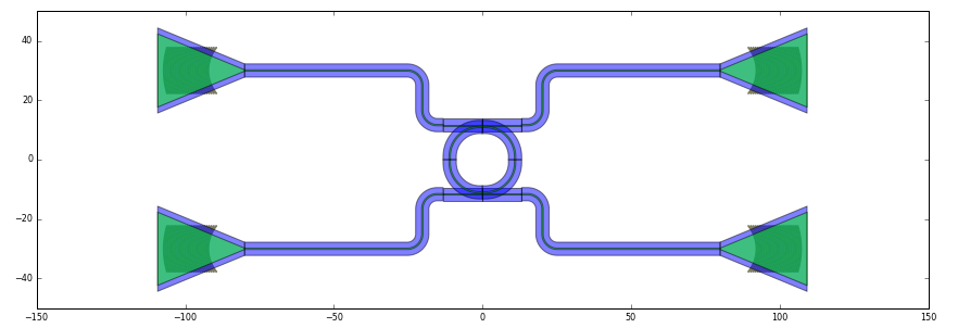
Layout of a ring resonator connected to grating couplers.
CircuitModel
The circuit model of an i3.Circuit is automatically composed from the circuit models of all of its subcomponents.
The default simulation model of the waveguide extracts its length from the layout. This is a very powerful technique in IPKISS; this means you can run post-layout simulations to get an accurate representation of the circuit behavior, taking into account layout-dependent properties of the system.
my_circuit_cm = my_circuit.CircuitModel()
wavelengths = np.linspace(1.50, 1.6, 2001)
S = my_circuit_cm.get_smatrix(wavelengths=wavelengths)

# 7. Plot
plt.figure()
plt.plot(wavelengths, np.abs(S['in', 'pass'])**2, 'b', label="pass")
plt.plot(wavelengths, np.abs(S['in', 'drop'])**2, 'r', label="drop")
plt.plot(wavelengths, np.abs(S['in', 'add'])**2, 'g', label="add")
plt.plot(wavelengths, np.abs(S['in', 'in'])**2, 'k', label="reflection")
plt.legend()
plt.show()
In the simulation, you clearly see the interference fringes that are obtained due to the reflections in grating couplers. The period of those fringes is based on the distance between the grating couplers and that information is obtained form the LayoutView. If you modify your layout - the simulations will follow accordingly.
Note
The terms of our circuit component (these are all the terms that are not connected) are exposed and renamed by i3.expose_ports) in _generate_ports.
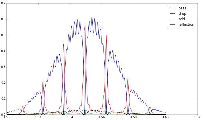
Transmission and reflection spectra of a ring resonator connected to grating couplers, obtained by circuit simulation.
You have just finished your first tutorial!
Recap
In this tutorial you learned how to assemble a circuit based on existing Picazzo components. You can also learn how to write your own (hierarchical) components from scratch. This is the subject of the next tutorials.