Logo
IPKISS 3.9

IPKISS

  • Installation
    • System Requirements
      • IPKISS Link for Siemens EDA
      • IPKISS Link for Ansys Lumerical
      • IPKISS Link for Dassault Systèmes Simulia
    • Installing IPKISS on Windows
      • Downloading the software
      • Installing the software
        • License types
        • Obtaining and installing a license
      • License Troubleshooting
      • Luceda Control Center
      • Installing a code editor
    • Installing IPKISS on Linux
      • Installing miniconda on Linux
      • Installing IPKISS packages
      • Installing the license on Linux
      • Configuring your IDE
    • Using a floating license
      • Hosting the license server
      • Configure your floating license
    • Installing a GDSII viewer
    • Where to go next
    • For IPKISS Link for Siemens EDA Users
      • Installing IPKISS Link for Siemens EDA
      • Verify your installation
    • Environment variables used by IPKISS
  • Tutorials
    • Introduction to Python
      • Python essentials
        • Variables
        • Lists and arrays
        • Loops
        • Functions
        • Loading modules
      • Object Oriented Programming in Python
        • What is object oriented programming
        • Object Oriented Programming in Python
        • Inheritance
        • Intermezzo: plotting in Python
        • Using your classes
      • Advanced class features
        • Private methods
        • Operator overloading
      • Finishing the sample program
        • Adding the Noisy Signal class
        • Implementing the filter class
        • Adjusting the main file
    • Setting up the environment
      • Downloading & installing Python editor
        • Launching PyCharm
      • IPKISS sample project
        • Setting up the interpreter
      • Create a new IPKISS design project
        • Configuring PyCharm
        • Adding a PDK
        • Adding a user library
        • Creating a new design
      • Some useful PyCharm features
        • Autocompletion
        • Jump-to-definition
        • Debugging
        • Configuring Python interpreter after project creation
      • Managing conda virtual environments and installing extra packages
        • Creating a development environment
        • Installing extra packages
      • Setting up the editor environment in Wing IDE
        • Creating a new project and choosing the python executable
        • The editor environment
        • Adding a folder to the project
        • Executing your first file
    • Quickstart: First simple circuit design
      • Step 1: Creating the components
        • The technology file
      • Step 2: Building circuits
        • Making the building blocks
        • Layout
        • CircuitModel
    • Design concepts
      • PCell and Views
      • Atomic Cell
      • Circuit (aka hierarchical cell)
        • Child and parent cells
        • Instances
        • Exposed ports
        • Placement & routings specifications
    • What is IPKISS?
      • Python Scripting
      • History
    • Ipkiss 3 overview
      • Ipkiss framework
        • Properties
        • PCell framework
        • Geometry
        • Layout
        • Netlist
        • Circuit simulation
        • Technology
        • Traces and waveguides
        • Virtual fabrication
        • Visualization
        • Device simulation
      • Picazzo component library
    • Layout: basics
      • Drawing waveguides
      • Creating a PCell
      • Building a small circuit
        • Ignore errors in specs
      • Parametrize cell and reuse
        • Parametrize spiral length
        • Parametrizing the trace template
        • Parametrizing the directional coupler
      • Verifying your layout
        • Netlist extraction
      • Post-layout simulation
      • Where to go from here
    • PCell: Basics
      • Step 1: PCell and Properties
        • The very beginning
        • Using properties to specify the design parameters
        • Executing a first script
        • Recap
      • Step 2: PCell and Views
        • Views
        • Instantiating views
        • Recap
      • Step 3: Technology
        • Using technology
        • Selecting a technology
        • Recap
      • Step 4: Simple layout: First GDSII
        • Adding elements to a layout
        • Visualizing and export to GDSII
        • Recap
    • Layout: Advanced (hierarchy and waveguides)
      • Step 1: Layout level hierarchy: Two Rings
        • Using ChildCellProperty to create Hierarchical PCells
        • Placing layout instances
        • Instantiating a hierarchical cell
        • Using defaults
        • Caution setting properties of child cells of TwoRingsWithDefaults
        • Recap
      • Step 2: Using waveguides in a layout
        • Waveguides
        • Default waveguide template and ChildCells
        • Placing the waveguides in the Layout View
        • Instantiating the ring
        • Modifying the width of the waveguide template
      • Step 3: Using ports and routes
        • Defining ports to connect components together
        • Using Routes
        • Defining the directional coupler using routes
        • Recap
      • Step 4: Using rounded waveguides
        • Defining rounded waveguides
        • Recap
    • Circuit models: Basics
      • First example of a model
      • Defining the CircuitModel view
      • Building a custom CompactModel
      • Building a circuit
      • Adding time-domain behavior
      • Writing multimode models
      • Specifying default values for parameters
      • Accessing the layout from the model view
      • Running simulations
        • Running a frequency-domain simulation
        • Running a time-domain simulation
      • Additional resources
    • Circuit models: Advanced
      • Model definition guidelines
      • Debugging Models
      • Python Models
      • Polynomial dependent variables and coefficients
      • Writing a netlist manually
      • Troubleshooting
    • Circuit models based on S-parameter data
      • Loading from touchstone into SMatrix1DSweep
        • Specific 3rd party tool support
      • Saving S-matrices to a TouchStone file
      • Creating a B-Spline interpolation model
      • Assigning an smatrix model to your PCell
    • Physical device simulation
      • General concept
      • The basic steps
      • Define the Simulation Geometry
        • Create a layout
        • Verifying the device geometry
        • Simulation Geometry
        • Advanced geometry settings
      • Choose a simulation tool
    • Building an Aperture
      • Implementing StripAperture
      • RibAperture
      • Simulation
        • Defining SlabModes
        • Defining a custom SlabTemplate
        • Customizing Field Calculation
  • Sample gallery
    • A Ring Resonator based Filter based on the Vernier principle
      • Defining the Vernier Filter Circuit
        • Component synthesis by defining a design algorithm
      • Running the design, simulation and layout
    • Make a Rectangular AWG
      • Getting started
      • The aperture
      • The input star coupler
      • The output star coupler
      • The rectangular waveguide array
      • The Arrayed Waveguide Grating
      • Running the Caphe simulation
      • Using SpectrumAnalyzer to analyze the results
    • SpectrumAnalyzer: Near and Far Crosstalk
      • The Spectrum Analyzer
      • Peaks per channel
      • Near and Far Crosstalk
    • Make a S-shaped AWG
      • Getting started
      • The aperture
      • The input star coupler
      • The output star coupler
      • The S shaped waveguide array
      • The Arrayed Waveguide Grating
      • Running the Caphe simulation
    • Loading a touchstone file
      • See also
    • Fixing sharp angles in the layout of a directional coupler
    • Creating a Cell from an Existing GDSII file
      • Export a grating coupler to GDSII
      • Importing the GDSII file
    • Disk Resonator with Wraparound waveguide
      • Defining the Parametric Cell
      • Generating the Disk Layout using geometric primitives
      • Creating a Waveguide child cell
        • Creating a Rounded Waveguide
        • Calculating the correct control shape
        • Using Waveguide Templates
        • Adding Ports
        • Recap
    • Running a CAMFR simulation to compute the field profiles
      • Getting started
      • Defining the technology Materials and Virtual Fabrication
      • Mapping the material stacks
      • Defining the layout
      • Defining the CAMFR simulation
      • Running the CAMFR simulations
      • Visualizing the simulation data
    • Defining a customized technology
      • Getting started
      • Adding a process layer
      • Defining rules
      • Visualization and import/export settings
      • Overwriting technology keys
      • Example: ring resonator with back-end opening cover layer
      • Defining the virtual fabrication
    • Creating a Cell from an existing GDSII file with a new technology
      • Adding the missing layers to a tech file
      • Importing a cell with GDSII layers in the new tech file
    • Spiral with Tapered Waveguides and Spline Bends
      • Defining the Spline Rounding Algorithm
      • Defining the trace template
      • Defining a spiral
    • Layout and simulation of a ring resonator with grating couplers
      • Importing the technology file
      • Creating the ring resonator
      • Running a circuit simulation
      • Creating the grating coupler
      • Creating a small circuit with the ring and grating coupler
    • Modifying the GDSII table of an existing technology
    • Netlist extraction from layout
      • Importing the technology file
      • Creating a MZI in layout
      • Extracting the netlist
      • Run a simulation
    • Simulating an aperture with CAMFR
      • Getting started
      • The aperture
      • Get the field profile at the aperture
      • CircuitModel: Check the backreflection of the aperture
  • Guides
    • Technology
      • General structure of a TECH-tree
      • Required technology tree
      • Write your own TECH: Recommended file structure
      • Name of the technology
      • Metrics
      • Process
      • GDSII
      • Display Settings
      • Design Rules
      • Materials
      • Virtual Fabrication
        • Mask layers
        • From mask layers to material stacks
      • Traces
      • Grating Couplers
      • OpenAccess (IPKISS Link for Siemens EDA only)
        • Layer settings
        • Routing settings
      • Required Technology Keys: IPKISS
      • Required Technology Keys: PICAZZO
    • Properties
      • DefinitionProperty
        • Using DefinitionProperty
        • Default Values
        • Restrictions
        • Preprocessors
      • Caching
      • Derivates of DefinitionProperty
    • Parametric Cells
      • IPKISS PCells
        • Properties
      • Views
        • Define the state of a View
        • Only one view instance per view class.
        • Retrieving Views
        • View property defaults
      • Making Fixed (P)Cells
      • IPKISS Views
      • Ports and terms
        • Port/term naming conventions
    • The Layout View
      • Layout concepts
      • Defining the layout view
      • Shapes
      • Elements
        • Boundary and Path elements
        • PolygonText
      • Groups
      • Using shape operations
      • Working with process purpose layers
      • Defining ports
      • Adding instances
      • Layout view inheritance
    • Hierarchical PCells
      • ChildCells
      • ChildCellProperty
      • Adding the child views
      • Overriding views originating from ChildCellProperty
      • Caution setting properties of child cell
    • Netlist
      • What is a Netlist view
      • Netlist terms
      • Netlist instances
      • Netlist Links
      • Naming of terms, links and instances
      • Generate a NetlistView from a LayoutView
        • Basic use
        • Generating terms only
        • Full hierarchical extraction
    • Waveguides
      • Waveguides are cells
      • Waveguides are Traces
      • Trace Templates
      • Predefined waveguide templates
      • How to use waveguides in a circuit (IPKISS)
      • How to use waveguides in a circuit (IPKISS Link for Siemens EDA module)
      • Basic waveguide example
      • See also
    • Caphe introduction
      • Circuit simulations
      • Building blocks for circuit simulations
      • Running circuit simulations in IPKISS
      • Advantages of using Caphe
      • Further reading
    • Boolean Operations
      • Booleans between Shapes
      • Booleans between Elements
        • Operations including Paths
      • Booleans between Layers
      • Booleans between ElementLists
      • A real-world example
  • IPKISS Reference
    • PCell Reference
      • PCell
      • Defining new Types with Properties
        • StrongPropertyInitializer
        • Adding Restrictions
        • Defining Default Values
        • Allowing None as a valid value
        • Caching
        • Locking Properties
        • Preprocessors
        • Documenting Properties
      • Properties & Restrictions Reference
        • Basic Properties
        • Properties Derived From DefinitionProperty
        • Restrictions
        • Property Preprocessors
        • Property Validation Errors
      • Library
    • Netlist Reference
      • Netlist view building blocks
        • NetlistView
        • Terms
        • Instances
        • Nets
      • Netlist extraction
        • NetlistFromLayout
        • extract_terms
    • Layout Reference
      • Geometry Reference
        • Coordinates
        • Basic Shapes
        • Spline Shapes
        • Shape modifiers
        • Rounding algorithms
      • Ports Reference
        • Optical Ports
        • Electrical Ports
        • Create Ports
      • Placement and Routing Reference
        • Functions and classes
        • Specifications
        • Route control
      • Routing
        • Routing types
        • RouteToLine
        • RouteToAngle
        • Helper Functions
      • Transformations
        • IdentityTransform
        • Translation
        • Rotation
        • VMirror
        • HMirror
        • CMirror
        • Stretch
        • Magnification
        • NoDistortTransform
      • Elements and Layers
        • Shape Elements
        • Reference Elements
      • SizeInfo
        • SizeInfo
        • Retrieving the size info
        • Operations
      • Importing Layouts from GDSII
        • GDSCell
      • Exporting Layouts to GDSII
        • write_gdsii
        • FileOutputGdsii
      • IoColumn
      • Layout View
      • Layout Operations
        • Boolean operations
        • Element operations
        • Layout operations
    • Connector Reference
      • Creating a connector
      • Connector algorithms
        • Connector
        • ConnectManhattan
        • ConnectManhattanTapered
        • ConnectBend
        • ConnectLogical
        • ConnectManhattanBundle
        • SBendFanout
    • Traces
      • Optical
        • WindowWaveguideTemplate
        • TraceTemplate
        • Waveguide
        • RoundedWaveguide
        • TaperedWaveguide
        • TaperedWaveguideTemplate
        • Using maximum bend radius
      • Bundles
      • Transitions
        • Waveguide transitions
        • Waveguide transitions starting from a port
        • AutoTraceTransitionFromPort
      • Electrical
        • ElectricalWire
        • ElectricalWireTemplate
        • ElectricalWindowWireTemplate
        • Electrical Vias
    • CircuitModel View reference
      • Instances of CircuitModelView
      • Defining and testing models and model view
        • CircuitModelView
        • CompactModel
        • HierarchicalModel
        • Probe
        • FunctionExcitation
        • SMatrix1DSweep
        • BSplineSModel
        • test_circuitmodel
        • map_terms
      • Numerical analysis
        • polyval
      • Spectrum analysis
        • SpectrumAnalyzer
        • Spectrum
        • spectrum_peaks
        • signal_power
        • signal_power_dB
        • find_peaks
        • find_peaks_spline
        • find_peaks_cwt
    • Device simulation reference
      • IPKISS
        • camfr_guided_modes
        • camfr_mode_fields
        • camfr_compute_stack_neff
        • camfr_stack_expr_for_structure
        • get_material_stacks
        • ipkiss3.all.device_sim.SimulationGeometry
        • ipkiss3.all.device_sim.SMatrixOutput
        • ipkiss3.all.device_sim.MacroOutput
        • ipkiss3.all.device_sim.FileOutput
        • ipkiss3.all.device_sim.Port
        • ipkiss3.all.device_sim.Macro
        • ipkiss3.all.device_sim.MacroFile
      • Vendor specific references
    • Technology Reference
      • Technology
        • get_technology
        • TechnologyTree
        • DelayedInitTechnologyTree
      • Process
        • ProcessLayer
        • PatternPurpose
        • ProcessPurposeLayer
        • PPLayer
        • Layer
      • GDSII
        • AutoGdsiiLayerInputMap
        • AutoGdsiiLayerOutputMap
        • GenericGdsiiPPLayerInputMap
        • GenericGdsiiPPLayerOutputMap
        • UnconstrainedGdsiiPPLayerInputMap
        • UnconstrainedGdsiiPPLayerOutputMap
      • Display
        • DisplayStyle
        • DisplayStyleSet
        • CyclicDisplayStyleSet
      • Materials
        • Material
        • MaterialFactory
        • MaterialStack
        • MaterialStackFactory
      • Virtual Fabrication
        • VFabricationProcessFlow
        • visualize_2d
        • cross_section
      • Example
    • File input/output
      • Touchstone import
        • import_touchstone_smatrix
      • Touchstone export
        • export_touchstone_smatrix
    • PDK structure
      • PDK Source and distributable PDK
      • Requirements for IPKISS Link for Siemens EDA
        • PDK Source requirements
        • Distributable PDK requirements
        • Config File (pdkname.cfg)
        • Contents File (all.py)
        • Technology File (pdkname.technology)
    • Indices and tables
  • Compact Models Reference
    • List of models
      • WG1
      • WG2
      • DC1
      • GC1
      • REFL1
    • Conventions
    • Using the models
  • Picazzo Reference
    • Logical Blocks
      • Logical Couplers
        • Coupler2x1
        • Coupler1x2
        • Coupler2x2
      • Model Parameters
      • Logical Inline Reflectors
        • Reflector
        • WaveguideReflector
      • Model
      • Logical Termination
        • Termination
        • PerfectTermination
    • Fiber Couplers
      • Curved Fiber Couplers
        • FiberCouplerCurvedGrating
        • FiberCouplerCurvedGratingGeneric
      • Uniform Line Fiber Couplers
        • UniformLineGrating
      • Fiber Coupler base classes
        • FiberCouplerGrating
    • Filters
      • Mach-Zehnder Interferometers
        • MZI
        • MZIWaveguides
        • MZIWithCells
        • MZIWaveguideArm
        • MZIContainerArm
      • Ring Resonators
        • Hierarchy of the ring circuit and layout
        • Coupler sections
        • Coupler positioning
        • Circuit model
      • Multi Mode Interferometers
        • Tapered MMIs
        • Untapered MMIs
        • Rib MMIs
    • Photonic Crystals
      • Generic Photonic Crystals
        • PhCLayout
        • DodecPhCLayout
        • HexPhCLayout
        • OctPhCLayout
        • SquarePhCLayout
        • TriangularPhCLayout
        • RectangularPhCLayout
      • Photonic Crystal W1 Waveguides and Cavities
        • GenericW1Waveguide
        • W1Waveguide
        • W1WaveguideWithInlineCavity
        • W1WaveguideWithAllpass
      • Photonic Crystal HeteroWaveguide Layouts
        • W1HeteroCavity
        • W1HeteroCavity1Mirror
        • W1HeteroCavityMulti
    • Traces
      • Wire Waveguides
        • WireWaveguideTemplate
        • Transitions
      • Rib Waveguides
        • RibWaveguideTemplate
        • RibWireWaveguideTemplate
        • Transitions
      • Thinned Waveguides
        • ThinnedWaveguideTemplate
        • Transitions
      • Slot Waveguides
        • SlotWaveguideTemplate
        • DoubleSlotWaveguideTemplate
        • Transitions
      • Socket Waveguides
        • SocketWaveguideTemplate
        • SlottedSocketWaveguideTemplate
        • Transitions
      • Electrical Wire
        • ElectricalWireTemplate
      • Transitions
        • Transition circuit models
    • Waveguide Blocks
      • Waveguide Bends
        • WgBend
        • WgBend90
      • Waveguide Splitters
        • WgYSplitter
        • WgYCombiner
        • WgY90Splitter
        • WgY90Combiner
        • WgY180Splitter
        • WgY180Combiner
      • Directional Couplers
        • StraightDirectionalCoupler
        • BendDirectionalCoupler
        • SBendDirectionalCoupler
        • CircuitModel details
      • Waveguide Crossings
        • WgDirectCrossing
        • WgParabolicCrossing
      • Waveguide Gratings
        • WaveguideNonUniformGrating
        • WaveguideUniformGrating
        • WaveguideSectionsGratingPeriod
        • ModifiedWaveguideGratingPeriod
        • WaveguideSideGratingPeriod
        • WaveguideSideRibGratingPeriod
        • WaveguideSideBlockGratingPeriod
        • WaveguideGrooveGratingPeriod
        • Model details
      • Waveguide Bundles
        • WaveguideBundle
        • TemplatedWaveguideBundle
      • Spirals
        • SingleSpiral
        • SingleSpiralRounded
        • DoubleSpiral
        • DoubleSpiralRounded
        • DoubleSpiralWithInCoupling
        • DoubleSpiralWithInCouplingRounded
        • FixedLengthSpiral
        • FixedLengthSpiralRounded
      • Waveguide Connectors
        • WaveguideConnector
        • RoundedWaveguideConnector
    • Routing
      • Placement and routing
        • ConnectComponents
        • PlaceAndConnect
    • Apertures
      • OpenAperture
      • WireWgAperture
    • Containers and Adapters
      • AutoTransitionPorts
        • AutoTransitionPorts
      • ExtendPorts
        • ExtendPorts
      • FanoutPorts
        • FanoutPorts
      • IoFibcoup
        • IoFibcoupGeneric
        • IoFibcoupEastWest
        • IoFibcoup
      • Containers with Waveguides
        • ContainerWithWaveguides
        • ContainerWithWaveguideBundle
        • ContainerWithRoundedWaveguides
        • ContainerWithRoundedWaveguideBundle
      • Route Ports
        • RoutePortsEastWest
        • RoutePortsAroundCorner
      • TerminatePorts
        • TerminatePorts
    • Electrical Components
      • Vias
        • ContactHole
        • Via12
    • Modulators
      • Phase modulators
        • Phase modulator trace templates
        • Phase modulator
    • single page reference
      • Logical Blocks
        • Coupler1x2
        • Coupler2x1
        • Coupler2x2
        • Reflector
        • WaveguideReflector
        • Termination
        • PerfectTermination
      • Grating Couplers
        • FiberCouplerCurvedGrating
        • FiberCouplerCurvedGratingGeneric
        • UniformLineGrating
        • FiberCouplerGrating
      • Ringresonators
        • RingRect
        • RingRect180DropFilter
        • RingRoundedShape
        • RingRectNotchFilter
        • RingRect180DropFilter
        • RingRect90DropFilter
        • RingRectWrappedNotchFilter
        • RingRectWrapped180DropFilter
        • RingRectSymmNotchFilter
        • RingRectSymm180DropFilter
        • RingRectSymm90DropFilter
        • RingRectSBendNotchFilter
        • RingRectSBend180DropFilter
      • Multi-mode Interferometers
        • MMITapered
        • MMIIdenticalTapered
        • MMISymmetricTapered
        • MMI1x2Tapered
        • MMI2x1Tapered
        • MMI2x2Tapered
        • RibMMIIdenticalTapered
        • RibMMISymmetricTapered
        • RibMMI1x2Tapered
        • RibMMI2x1Tapered
        • RibMMI2x2Tapered
        • MMI
        • MMIIdentical
        • MMISymmetric
        • MMI1x2
        • MMI2x1
        • MMI2x2
      • Mach-Zehnder Interferometers (MZI)
        • MZI
        • MZIWaveguides
        • MZIWithCells
        • MZIWaveguideArm
        • MZIContainerArm
      • Generic Photonic Crystals
        • DodecPhCLayout
        • HexPhCLayout
        • OctPhCLayout
        • SquarePhCLayout
        • TriangularPhCLayout
        • RectangularPhCLayout
      • Photonic Crystal HeteroWaveguide Layouts
        • W1HeteroCavity
        • W1HeteroCavity1Mirror
        • W1HeteroCavityMulti
      • Photonic Crystal W1 Waveguides and Cavities
        • GenericW1Waveguide
        • W1Waveguide
        • W1WaveguideWithInlineCavity
        • W1WaveguideWithAllpass
      • Rib Waveguides
        • RibWaveguideTemplate
        • RibWireWaveguideTemplate
      • Slot Waveguides
        • SlotWaveguideTemplate
        • DoubleSlotWaveguideTemplate
      • Socket Waveguides
        • SocketWaveguideTemplate
        • SlottedSocketWaveguideTemplate
      • Thinned Waveguides
        • ThinnedWaveguideTemplate
        • ThinnedWaveguideTemplate
      • Wire Waveguides
        • WireWaveguideTemplate
      • Rib Transitions
        • WireRibWaveguideTransitionLinear
        • WireRibWaveguideTransitionFromPortLinear
      • Slot Transitions
        • SlottedWireWaveguideTransitionLinear
        • SlottedWireWaveguideTransitionFromPortLinear
      • Socket Transitions
        • WireSocketWaveguideTransitionLinear
        • WireSocketWaveguideTransitionFromPortLinear
      • Thinned Transitions
        • ThinnedWireWireWaveguideTransitionLinear
        • ThinnedWireWireWaveguideTransitionFromPortLinear
      • Wire Transitions
        • WireWaveguideTransitionLinear
        • WireWaveguideTransitionFromPortLinear
      • Bends
        • WgBend
        • WgBend90
      • Crossings
        • WgDirectCrossing
        • WgParabolicCrossing
      • Gratings
        • WaveguideUniformGrating
        • WaveguideNonUniformGrating
        • ModifiedWaveguideGratingPeriod
        • WaveguideSideGratingPeriod
      • Directional Couplers
        • StraightDirectionalCoupler
        • BendDirectionalCoupler
        • SBendDirectionalCoupler
      • Splitters
        • WgYSplitter
        • WgYCombiner
        • WgY90Splitter
        • WgY90Combiner
        • WgY180Splitter
        • WgY180Combiner
      • Waveguide Bundles
        • WaveguideBundle
      • Spirals
        • SingleSpiral
        • SingleSpiralRounded
        • DoubleSpiral
        • DoubleSpiralRounded
        • DoubleSpiralWithInCoupling
        • DoubleSpiralWithInCouplingRounded
        • FixedLengthSpiral
        • FixedLengthSpiralRounded
        • ConnectComponents
        • PlaceAndConnect
        • OpenAperture
        • WireWgAperture
      • AutoTransitionPorts
        • AutoTransitionPorts
      • FanoutPorts
        • FanoutPorts
      • IoFibcoup
        • IoFibcoupGeneric
        • IoFibcoupEastWest
        • IoFibcoup
      • ContainerWithWaveguides
        • ContainerWithWaveguides
        • ContainerWithWaveguideBundle
        • ContainerWithRoundedWaveguides
        • ContainerWithRoundedWaveguideBundle
      • ExtendPorts
        • ExtendPorts
      • Route Ports
        • RoutePortsEastWest
        • RoutePortsAroundCorner
      • TerminatePorts
        • TerminatePorts
        • ContactHole
        • Via12
      • Phase Modulators
        • PhaseShifterWaveguideTemplate
        • LateralPNPhaseShifterTemplate
        • LongitudinalPNPhaseShifterTemplate
        • PhaseModulator

Modules

  • IPKISS AWG Designer
    • Getting Started
      • 1. PDK setup
      • 2. Reviewing the subcomponents
      • 2. Synthesize the AWG device
      • 3. Implement the AWG
      • 4. Preparing for tape-out
      • 5. Incorporating into a circuit
    • Guides
      • AWG Components
        • Overview
        • Slab Template
        • Apertures
        • Star Coupler
        • Waveguide Array
      • AWG Simulation
        • High-level AWG simulation strategy
        • Star coupler simulation
        • Waveguide array simulation
    • API Reference
      • AWG Components
        • Slab templates
        • Apertures
        • Star couplers
        • Waveguide Array
        • Arrayed Waveguide Gratings
      • Functions
        • Design
        • Field profiles
        • Layouting
        • Analysis (deprecated)
        • Utilities
        • Legacy methods
  • IPKISS IP Manager
    • Features
    • User Manual
      • Introduction
        • Component reference tests
        • Getting started
      • Getting started: defining tests for a library
        • Example project
        • Adding tests to the library
        • Generating the known-good reference files
        • Running tests
        • HTML output
        • Changing library components or their tests
      • Getting started: increasing test coverage
        • Add a circuit model reference test
        • Add a layout-versus-netlist test
        • Sharing settings across tests
        • Add your own circuit checks
      • Advanced features and options
        • Test parametrization
        • S-model testing
        • Specify which tests to run
        • Use a different path for the reference or temporary files
        • Specify timestamp in GDS files
      • IP Manager Reference
        • Test classes
        • Component reference tests
        • Helper classes
        • Functions

Links

  • IPKISS Link for Siemens EDA
    • Working with IPKISS Link for Siemens EDA
      • Getting started with IPKISS Link for Siemens EDA
        • Installing a license file
        • Using the example library
        • Starting L-Edit
        • Loading the demonstration project
      • Creating a new design based on a PDK
        • Step 1: Start a new design
        • Step 2: Instantiate cells
        • Step 3: Route and generate waveguides
        • Step 4: Adapt waveguide routes
      • Reusing cells in circuits
        • Create the MZI design
        • Create the test design
        • Conclusion
    • Library organization
      • Step 1: The PDK
      • Step 2: User libraries
      • Step 3: Designs in IPKISS (code-based)
      • Step 4: Designs in IPKISS (OpenAccess based)
      • Step 5: Exporting user libraries to OpenAccess
    • Known limitations and issues
      • Limitations
      • Issues
    • Logging configuration
      • File logging
        • Loglevel
        • Logfolder location
  • IPKISS Link for Ansys Lumerical
    • Tutorial FDTD
      • 1. Define the geometry
      • 2. Define the simulation
      • 3. Inspect the simulation job
      • 4. Retrieve and plot simulation results
      • 5. Advanced simulation settings
        • Monitors
      • 6. Tool-specific settings
        • Using materials defined by the simulation tool
        • Macros
        • Export additional settings from Lumerical FDTD to IPKISS
    • Tutorial EME
      • 1. Define the geometry
      • 2. Define the simulation
      • 3. Inspect the simulation job
      • 4. Retrieve and plot simulation results
      • 5. Advanced simulation settings
        • Monitors
      • 6. Tool-specific settings
        • Using materials defined by the simulation tool
        • Macros
        • Export additional settings from Lumerical EME to IPKISS
    • API Reference
      • ipkiss3.all.device_sim.SimulationGeometry
      • ipkiss3.all.device_sim.SMatrixOutput
      • ipkiss3.all.device_sim.MacroOutput
      • ipkiss3.all.device_sim.FileOutput
      • ipkiss3.all.device_sim.Port
      • ipkiss3.all.device_sim.Macro
      • ipkiss3.all.device_sim.MacroFile
      • ipkiss3.all.device_sim.LumericalFDTDSimulation
      • ipkiss3.all.device_sim.LumericalEMESimulation
      • Macros
        • fdtd_profile_xy
        • fdtd_mesh_accuracy
        • export_port_neff
        • eme_setup
        • eme_profile_xy
        • eme_transverse_mesh
        • eme_wavelength
  • IPKISS Link for Dassault Systèmes SIMULIA
    • Tutorial
      • 1. Define the geometry
      • 2. Specify the simulation job
      • 3. Inspect the simulation job
      • 4. Retrieve and plot simulation results
      • 5. Advanced simulation settings
        • Monitors
      • 6. Use tool-specific settings
        • Using materials defined by the simulation tool
        • Macros
        • Export additional settings from CST Studio Suite to IPKISS
        • Multiphysics simulations
    • API Reference
      • ipkiss3.all.device_sim.SimulationGeometry
      • ipkiss3.all.device_sim.SMatrixOutput
      • ipkiss3.all.device_sim.MacroOutput
      • ipkiss3.all.device_sim.FileOutput
      • ipkiss3.all.device_sim.Port
      • ipkiss3.all.device_sim.Macro
      • ipkiss3.all.device_sim.MacroFile
      • ipkiss3.all.device_sim.CSTTDSimulation
      • Macros
        • field_monitor

Support and Changelog

  • Release notes
    • Release notes IPKISS Photonics Design Platform 3.9.0
      • Python 3
      • IPKISS IP Manager stability
      • Touchstone exporter
    • Release notes IPKISS Photonics Design Platform 3.8.0
      • Introducing IPKISS IP Manager
      • Waveguide bundles
      • Spectrum Analysis
    • Release notes IPKISS Photonics Design Platform 3.7.1
      • Euler bends
      • Relative waypoints
      • Backward incompatibilities IPKISS 2.4
      • GDS export improvement
    • Release notes IPKISS Photonics Design Platform 3.7.0
      • Place and route of photonic ICs using i3.Circuit
      • Placing and routing
      • Connectors
        • Manhattan control points
      • Custom solver macros
    • Release notes IPKISS Photonics Design Platform 3.6.0
      • Device simulation (IPKISS Link for Ansys Lumerical)
      • Layout improvements
      • AWG Designer
      • Caphe
      • IPKISS Link for Siemens EDA
    • Release notes IPKISS Photonics Design Platform 3.5.0
      • IPKISS AWG Designer
        • Note on backward compatibility
      • Layout improvements
      • CAMFR improvements
    • Release notes IPKISS 3.4.0
      • Product structure
      • IPKISS.eda module
      • IPKISS
      • Documentation
    • Release notes IPKISS 3.3.0
      • Spec-based device placement
      • Netlist extraction
      • Documentation improvements
    • Release notes IPKISS 3.2.0
      • Physical device simulation links
      • Model building
      • Documentation improvements & new tutorials
    • Release notes IPKISS 3.1.3
      • New compact model framework
        • Redesigned model syntax
        • Adding circuit models to libraries and PDKs
        • Time-domain API
        • Overall improvements on the simulation side
      • Bundled editor
      • Custom routing in IPKISS.eda
    • Release notes IPKISS 3.1.2
      • Improvements to internal caching
      • Virtual fabrication
      • Using matplotlib notebook
    • Release notes IPKISS 3.1.1
      • License installation and verification
      • Updated packages
      • Visualization: ports can be labeled
      • Cross-sections of trace templates
      • PlaceAndConnect draws flylines when links are not properly connected
      • Shapes for performing spline fitting
        • ShapeFitNaturalCubicSpline
        • ShapeFitClampedCubicSpline
    • Release notes IPKISS 3.1.0
  • Changelog
    • IPKISS Photonics Design Platform
      • IPKISS Photonics Design Platform 3.9.0
        • General
        • IPKISS
        • IPKISS IP Manager
        • IPKISS AWG Designer
        • IPKISS Link for Siemens EDA
        • Documentation
      • IPKISS Photonics Design Platform 3.8.0
        • IPKISS
        • IPKISS AWG Designer
        • IPKISS IP Manager
        • Caphe
      • IPKISS Photonics Design Platform 3.7.1
        • IPKISS
      • IPKISS Photonics Design Platform 3.7
        • IPKISS
        • IPCORE
        • IPKISS AWG Designer
        • IPKISS Link for Ansys Lumerical
        • IPKISS Link for Dassault Systèmes Simulia
        • Documentation
        • Luceda Academy
      • IPKISS Photonics Design Platform 3.6
        • IPKISS
        • IPKISS Link for Ansys Lumerical
        • IPKISS Link for Dassault Systèmes Simulia
        • IPKISS Link for Siemens EDA
        • IPKISS AWG Designer
      • IPKISS Photonics Design Platform 3.5
        • Ipkiss
        • Picazzo
        • Documentation
        • IPKISS AWG Designer
    • Previous IPKISS versions
      • Ipkiss 3.4.1
        • Ipkiss
        • Ipkiss.eda
        • Documentation
      • Ipkiss 3.4
        • Installation
        • Ipkiss
        • Ipkiss.eda
        • Documentation
        • Backward compatibility notes
      • Ipkiss 3.3
        • Documentation
        • Ipkiss
        • Picazzo
        • Ipkiss.eda
      • Ipkiss 3.2.1
        • General
        • Ipkiss
        • Documentation
      • Ipkiss 3.2
        • General
        • Ipkiss
        • Ipcore
        • Caphe
        • Luceda control center
        • Ipkiss.eda
        • Documentation
      • Ipkiss 3.1.3
        • General
        • Ipcore
        • Ipkiss
        • Caphe
        • Picazzo
        • Ipkiss.eda
      • Ipkiss 3.1.2
        • Installation & Getting Started
        • Ipcore
        • Ipkiss
        • Pysics
        • Picazzo
        • Ipkiss.eda
        • Ipkiss 2.4 Compatibility
        • Documentation
      • Ipkiss 3.1.1
        • Ipkiss
        • Ipkiss-caphe interface
        • Picazzo
        • Samples & documentation
      • Ipkiss 3.1.0
        • Installation
        • Samples & documentation
        • Ipcore
        • Ipkiss
        • Picazzo
        • Picazzo 2.4
        • Ipkiss 2.4
        • Pysimul
      • Ipkiss 3.0.1
        • Ipcore
        • Ipkiss
        • Picazzo
        • Simulation
        • i-Python notebooks
        • Ipkiss 2.4 compatibility
      • Ipkiss 3.0
        • Functionality
        • User experience
        • Under the hood
      • Ipkiss 2.4.6
        • Ipkiss
        • Picazzo
        • Pysimul
      • Ipkiss 2.4.5
        • Ipkiss
        • Pysimul
        • Documentation
        • Picazzo
        • Spectral_toolbox
      • Ipkiss 2.4.4
        • Ipkiss
        • Ipcore
        • Picazzo
  • Backwards compatibility
    • Porting from Ipkiss 3.8 to Ipkiss 3.9 py3
      • Updating your code for IPKISS 3.9 py3
      • General Python 2 to Python 3 migration
        • Print
        • Division
        • Round
        • Ceil and floor
        • Imports relative to a package
        • Iterators
        • The __future__ module in Python
        • Unicode Support
        • More information
      • Python 2 to 3 code translation using 2to3
        • Using 2to3 in practice
      • PyCharm assistance to write Python 2 + Python 3 compatible code
      • Need support?
    • Known changes and backwards incompatibilities in 3.9.0
      • Deprecation LongIntProperty and removal of explicit long int
        • Deprecation of Python 2 division operator overloading (__div__, __idiv__ and __rdiv__)
        • IP Manager reference files
      • Picazzo containers netlist
        • Removal of ObserverList and EventList
      • Numpy 1.16
        • Removed symbols from i3
    • Porting from Ipkiss 3.7.1 to Ipkiss 3.8
      • Porting filter analysis functions
        • Example
    • Known changes and backwards incompatibilities in 3.8.0
      • Compact Models
      • Netlist extraction with array references
    • Porting from Ipkiss 3.7 to Ipkiss 3.7.1
      • Porting i3.Structure
      • InOpticalPort, OutOpticalPort removed
      • Optical and electrical plugins`
      • Electrical port list
      • Window waveguide definitions and windows
    • Known backwards incompatibilities in 3.7.0
      • Bend size calculation changes
      • RoundedWaveguide: bend radius verification
      • Straight section lengths in TaperedWaveguide
      • Order of placed instances
      • AWGDesigner: Straight section lengths in RectangularExpandedAWG
      • Removal internal_member_name
    • Porting from Ipkiss 3.6 to Ipkiss 3.7
      • Porting CircuitCell (Luceda Academy) to IPKISS 3.7
        • Porting simple cells
        • Porting parametric cells (inheritance)
      • Porting PlaceComponents/PlaceAndAutoRoute
      • Porting i3.place_insts
    • Known backwards incompatibilities in 3.6.0
    • Known changes in 3.6.0
      • Stubbing of acute angles
      • Tapered waveguide
      • AWG fanout in waveguide arrays
    • Known backwards incompatibilities in 3.5.0
      • Shape Cutting Algorithm
      • CAMFR Engine
    • Porting from Ipkiss 3.4 to Ipkiss 3.5
      • Replacing ExpandedWaveguide by TaperedWaveguide
      • IPKISS AWG Designer
        • Import statement
        • Apertures
        • Star Couplers
        • Arrayed Waveguide Gratings
        • CAMFR engine
        • PDKs
        • Other
    • Known backwards incompatibilities in 3.4.0
      • TraceBundle
      • IPKISS.eda
      • IPKISS.eda logging
      • Timestamps: created, modified
      • Unit and Grid Properties
      • Locked properties
    • Porting from Ipkiss 3.3 to Ipkiss 3.4
      • Rebuilding your libraries
      • PDK Config File
      • Routing functions
    • Known backwards incompatibilities in 3.3.0
      • NetlistFromLayout
      • Spirals
      • Autotransition database
    • Layout changes 3.2.0
      • ShapeArc
      • route_to_parallel_line
    • Known backwards incompatibilities 3.1.3
      • Waveguide circuit models
      • Subclassing legacy CapheModel
      • ShapeWindowTraceTransition.straight_extension
    • Porting circuit models and user code from Ipkiss 3.1.2 to Ipkiss 3.1.3
      • 1. Convert PCell definition
      • 2. Convert user code
    • Known backwards incompatibilities 3.1.2
    • Porting from Ipkiss 3.0.1 to Ipkiss 3.1
      • Luceda debug environment variables have changed
      • PICAZZO: The Transition between WireWaveguides has an adaptive length
      • PICAZZO: The default purpose of ElectricalWireTemplate has changed
    • Porting from Ipkiss 3.0 to Ipkiss 3.0.1
      • The set method is more restrictive
      • Casting of Numbers in NumberProperties
      • PortList behaves similar to TermDict
      • Layer Properties in PICAZZO
      • Technology
      • Explicit Evaluations of child views are no longer required
      • Notebooks are now using IPython 3
    • Running Ipkiss 2.4 code in Ipkiss 3
      • Property system
        • Using properties on objects that don’t inherit from StrongPropertyInitializer
        • Overriding Properties with normal python attributes
        • Implementing Restrictions
        • Creating classes with definition names that are not declared at first
        • Number properties are cast to the correct type
      • Leading and trailing underscores
      • Layout
        • Magnification
      • Technology files
      • Mixing 3.0 and 2.4 syntax
    • Porting from Ipkiss 2.4 to Ipkiss 3
      • Importing Ipkiss
      • Property defaults: define_ → _default_
      • Structure (2.4) → PCell/LayoutView (3.0)
      • Port names
      • Using the Layout view
      • Netlist View
      • Hierarchy
        • Default children
        • Passing parameters from parent to default child
      • Waveguide Definition (2.4) → Waveguide Template (3.0)
        • Custom window waveguide definitions (2.4) -> window trace templates (3.0)
        • WgElDefinition
      • Waveguides: cells instead of layout elements
      • Picazzo
      • Technology
  • Summary per version
  • Glossary
    • Design Automation
      • General
      • Semiconductor ecosystem
      • Layout and mask
      • Modeling
      • Formats
      • Verification
    • Photonics
    • IPKISS
    • Python Programming
  • Support
    • Who is entitled to support
    • Software
    • Purchasing
    • Licensing
    • Foundry Process Design Kits
    • Training
    • Troubleshooting
  • 🌐 lucedaphotonics.com
  • 🎓 academy.lucedaphotonics.com
IPKISS
  • »
  • IPKISS & L-Edit documentation »
  • Working with IPKISS Link for Siemens EDA »
  • Getting started with IPKISS Link for Siemens EDA

Getting started with IPKISS Link for Siemens EDA

Installing a license file

Make sure both the Tanner L-Edit and IPKISS licenses are working. Please refer to License types for full instructions on how to setup the licensing.

Note

OpenAccess databases

If this is your first time you use an OpenAccess (OA) enabled electronic design automation (EDA) tool, here is some terminology that you should be aware of:

OpenAccess (OA)

A standard interface for software tools to use IC design databases. OpenAccess is an application programming interface (API) to databases which hold design information, such as for electronic or photonic ICs. For instance, an OA database can contain technology settings, and different cells with layout data and schematic data, up to complete IC designs. OA allows different software tools to access such database through a standard. The demonstration libraries in this tutorial are OA libraries, generated by IPKISS, using the standard OA database implementation. You can see it as a collection of files representing technology and design information.

lib.defs

A file that describes the the name and location of each library included in an IC design project, supported by the major tools.

OpenAccess attached library

A library that is used as technology reference. The technology settings (layers, grid, database units) are loaded from this library. It may also contain a series of predefined components (grating couplers, waveguides, couplers, splitters, ring resonators, …).

Using the example library

A demonstration library and associated projects are included in the samples folder of your installation (typically under %USERPROFILE%\luceda\samples\ipkiss390). The organization of this library is explained in Library organization. Here, we just demonstrate how the library can be opened.

Starting L-Edit

The L-Edit / IPKISS integration will be loaded as soon as you open a library made with IPKISS. Therefore, you can just double-click on L-Edit in the start menu and open a library, or you can double-click on the lib.defs file of said library.

You can check if the integration is loaded by looking for the following message in the L-Edit console window.

L-edit / IPKISS integration message.

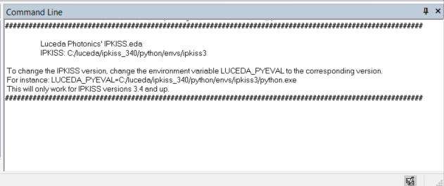
The L-edit / IPKISS integration message.

Note

The IPKISS version used in the integration is set using the environment variable LUCEDA_PYEVAL. This is normally set during the installation. To set or change the IPKISS version, change the environment variable to a different python executable. For instance:

LUCEDA_PYEVAL=C:/luceda/ipkiss_340/python/envs/ipkiss3/python.exe

This will only work for IPKISS versions 3.4 and up.

Loading the demonstration project

To load the demo project, we use File –> Open, and open the lib.defs project file from \demo\projects\my_designs_oa under the %USERPROFILE%\luceda\samples\ipkiss390 directory.

Open new design in L-Edit.

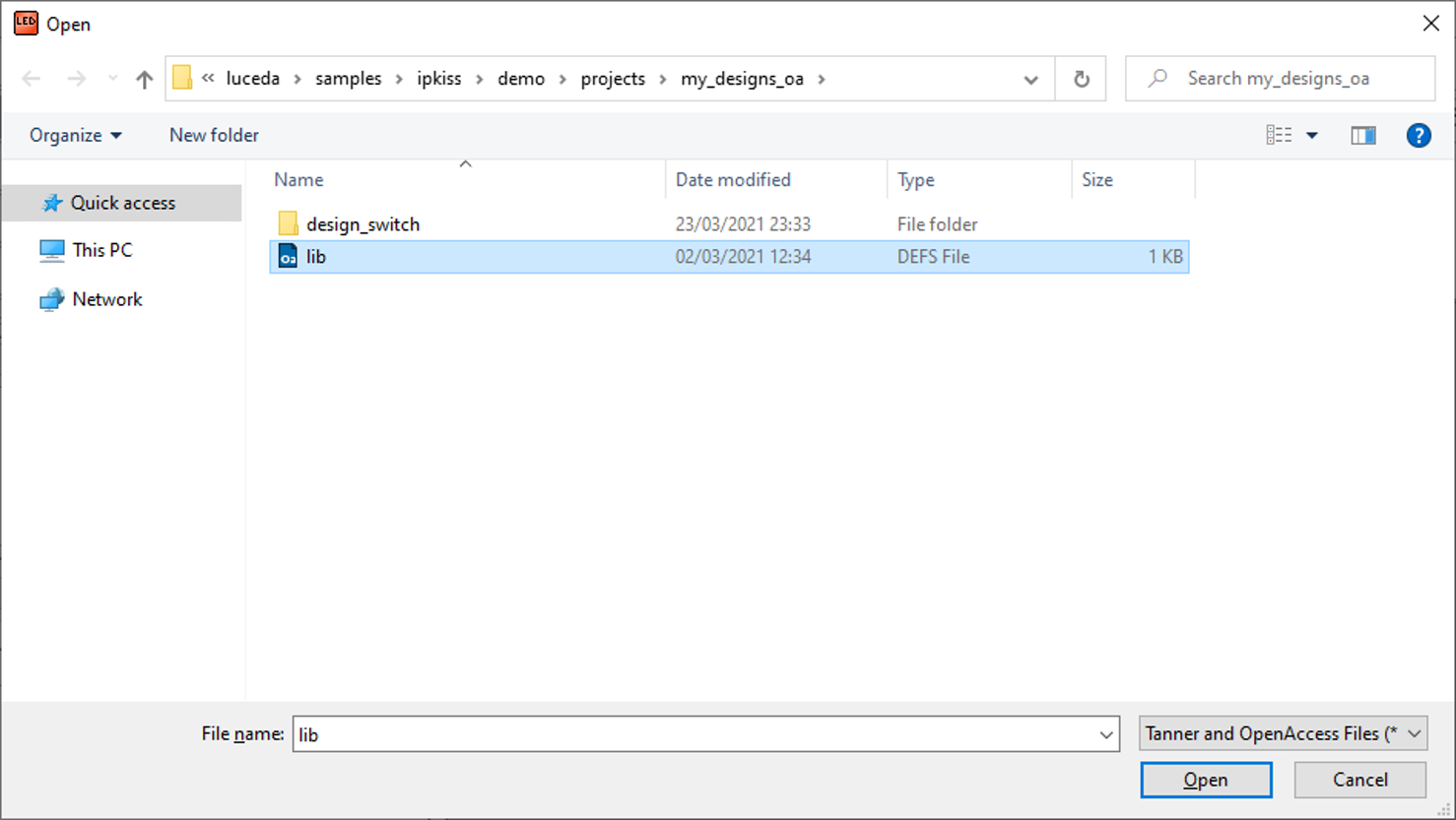
Open the demonstration project in L-Edit.

Select design_switch as the top-level library, and open one of the circuit examples.

Choose design_switch.

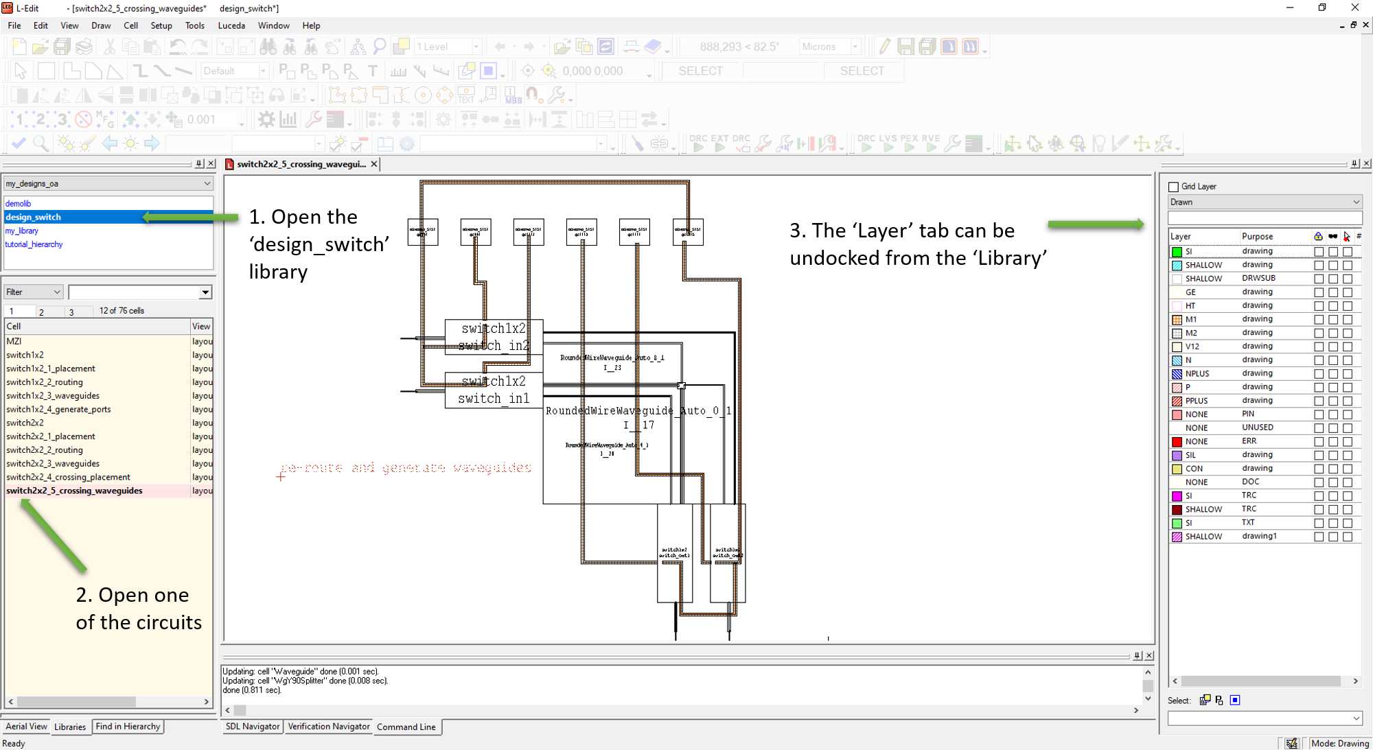
The demonstration project contains several libraries: the PDK (demolib), custom components (my_library), example design (design_switch) and a tutorial (see next chapter).

Note

IPKISS Link for Siemens EDA requires that the user’s main design is saved to an OA database. All libraries or PDKs exported by IPKISS Link for Siemens EDA’s pdktools are also OA databases. Cells from Tanner Database Files (.tdb) can still be instantiated.

Next Previous

© Copyright Luceda Photonics.

Built with Sphinx using a theme provided by Read the Docs.