Step 1: Creating the components
Result
We create the layout and circuit models for a ring resonator drop filter and a grating coupler. For this, we use pre-existing parametric building blocks that are defined in the Picazzo library.
Illustrates
how to import a technology file.
how to use the Layout of an existing component.
how to use the circuit model of an existing component.
How to run this example
To run the example, run execute_01_layout.py in the Python code editor of your choice.
The technology file
The first step in every design is to import the technology file. The technology contains a set of default values that characterize
the technology you will use to fabricate your chips. This technology file is typically provided by the fabrication facility (fab) you use.
Here we work with a generic silicon_photonics technology file, which is based on a standard SOI (silicon on insulator) process.
from technologies import silicon_photonics
from ipkiss3 import all as i3
Before we continue, we have to import some python libraries: numpy for array operations and matplotlib (through pylab) for plotting.
import numpy as np
import pylab as plt
As mentioned earlier, we use the IPKISS library Picazzo to create the building blocks of our circuit.
Of course it is also possible to build your own components from scratch, but a lot of commonly used photonic
components are already present in Picazzo, and variations of these components can already get you quite far.
Our first component is a RingRect180DropFilter, a ring resonator with two inputs and two outputs, that acts as
a wavelength channel add/drop filter.
The first step for using this component is to import it from the picazzo3 library and instantiate it.
from picazzo3.filters.ring import RingRect180DropFilter
my_ring = RingRect180DropFilter()
print my_ring
Here we created my_ring. my_ring is a PCell. A PCell is a container for all information on a component. This includes:
Properties: These are the parameters that you can set to modify the behavior of the PCell.
Layout : This is the view of a PCell which describes the mask layout of the cell. That layout is typically exported to a GDSII file. The Layout view can also contain properties which are relevant to the layout only.
CircuitModel : This is the view of a PCell which describes the compact model. This model can also contain properties that are relevant for the simulation only.
In what follows we will define two views on this ring resonator PCell: the Layout and the CircuitModel.
After completion of that process, our cell will have a Layout and a circuit model which we can reuse in a circuit.
Layout
We first instantiate the Layout of the PCell and set some of its properties. For the Layout of my_ring, we will set the bend_radius.
After creating the layout, we can visualize and/or export it to GDSII:
my_ring_layout = my_ring.Layout(bend_radius=10.0)
my_ring_layout.visualize()

my_ring_layout.write_gdsii("my_ring.gds")
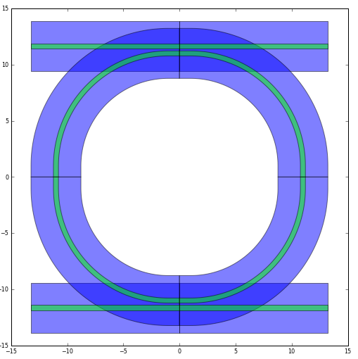
Layout of a ring_resonator.
We can also visualize our component in a GDSII viewer (here KLayout)
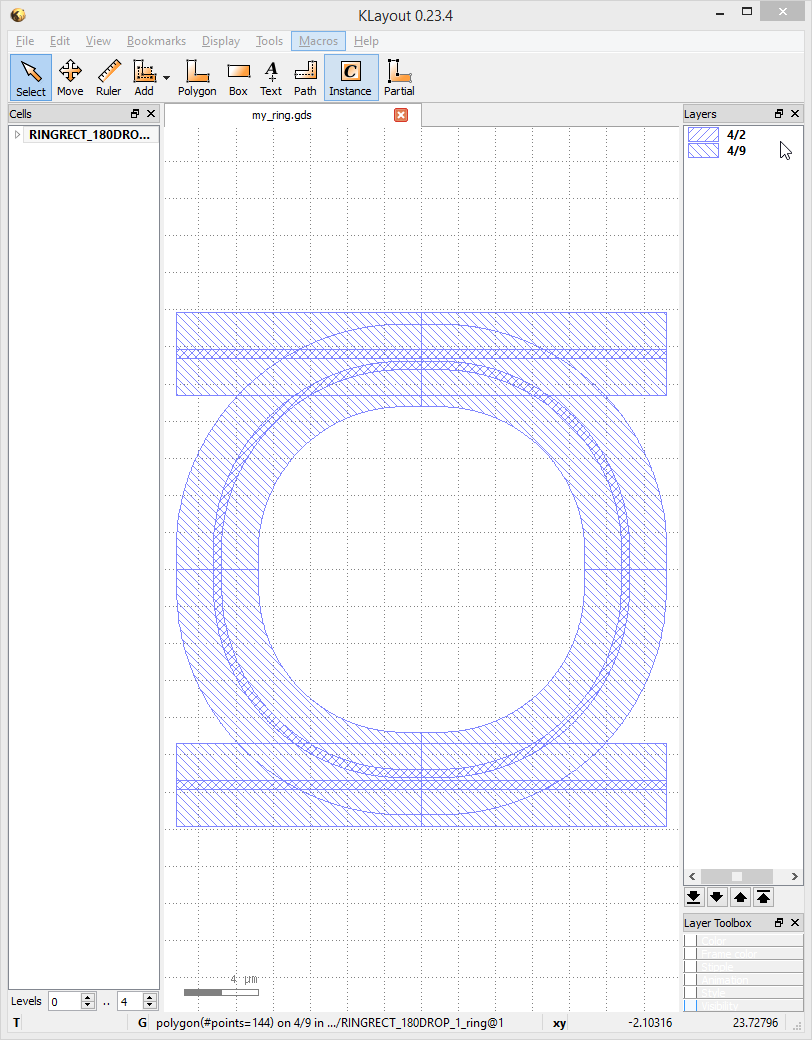
GDSII of a ring_resonator in KLayout.
CircuitModel
Each PCell can have an optical circuit model based on a scatter matrix. The behavior of that model can also be set through
properties. For my_ring the model of the ring is based on a composition of the directional coupler and the ring segments themselves.
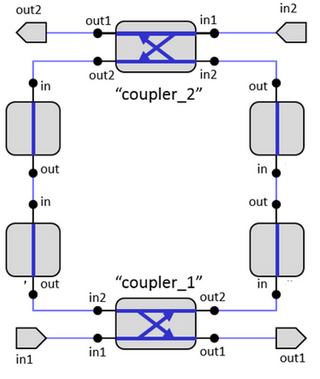
Circuit model of the ring
Therefore, the coupling parameters and ring length are relevant for the simulation. We set the relevant properties, start a simulation and plot the results.
Note: the first time, the simulation might be slow, because the circuit models are compiled in the background for optimal performance.
cp = dict(cross_coupling1=1j*0.3**0.5,
          straight_coupling1=0.7**0.5) #The coupling from bus to ring and back


my_ring_cm = my_ring.CircuitModel(coupler_parameters=[cp, cp])

wavelengths = np.linspace(1.50, 1.6, 2001)
S = my_ring_cm.get_smatrix(wavelengths=wavelengths)

plt.plot(wavelengths, np.abs(S['in1', 'out1'])**2, 'b', label="pass")
plt.plot(wavelengths, np.abs(S['in1', 'out2'])**2, 'r', label="drop")
plt.plot(wavelengths, np.abs(S['in1', 'in2'])**2, 'g', label="add")

plt.xlabel("Wavelength ($\mu m$)")
plt.ylabel("Power transmission")
plt.legend()
plt.show()
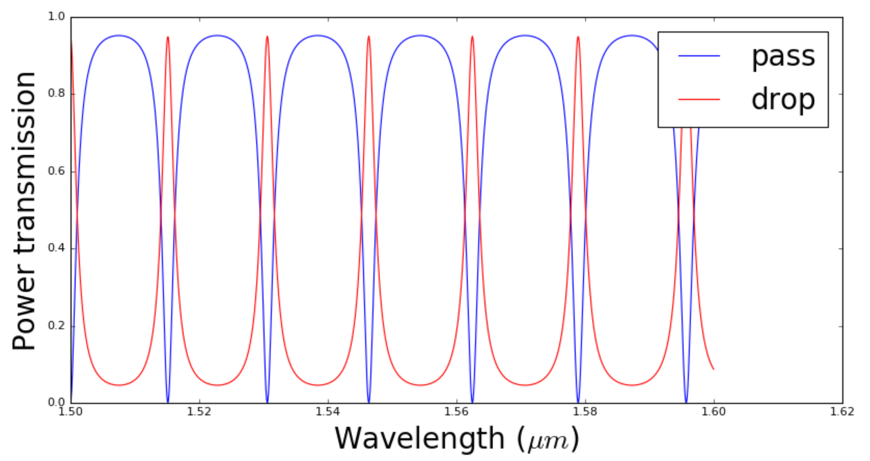
Simulation result of the ring resonator.
Grating Coupler
In this section we create a grating coupler. We load it from the Picazzo library, set the Layout and visualize it.
from picazzo3.fibcoup.curved import FiberCouplerCurvedGrating
my_grating = FiberCouplerCurvedGrating()

# 7. Layout
my_grating_layout = my_grating.Layout(n_o_lines=24, period_x=0.65, box_width=15.5)
my_grating_layout.visualize()
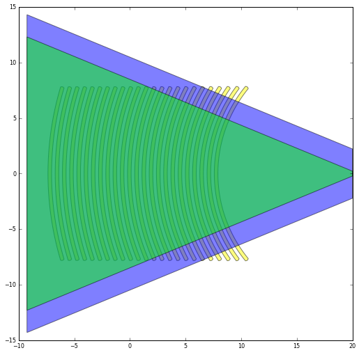
Layout of the grating coupler.
We also create set the CircuitModel of the grating coupler. This is a simple analytical model based on a peak transmission, a 3dB bandwith and reflection.
my_grating_cm = my_grating.CircuitModel(center_wavelength=1.55, bandwidth_3dB=0.06, peak_transmission=0.60**0.5, reflection=0.05**0.5)
S = my_grating_cm.get_smatrix(wavelengths=wavelengths)
plt.plot(wavelengths, np.abs(S['vertical_in', 'out'])**2, 'b', label="pass")
plt.legend()
plt.show()
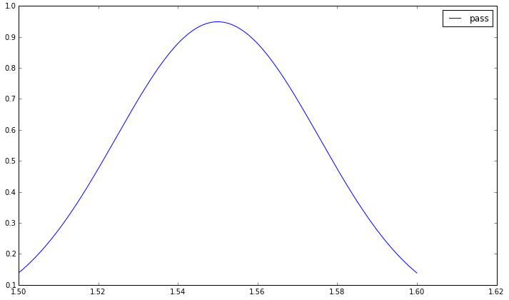
Transmission of the grating coupler as a function of wavelength.
Recap
In this step, we explained how to instantiate existing Picazzo components. In Step 2: Building circuits we will assemble them in a circuit.