Note
Click here to download the full example code
Netlist extraction from layout
In this example we build a circuit in layout, and extract the netlist so we can run circuit simulations.
Importing the technology file
We start with importing the demolib PDK technology, which is a basic PDK shipped with IPKISS. You can replace this by another PDK (custom made, or from our list of supported PDKs). and the layers will automatically adjust to reflect this technology.
from technologies.silicon_photonics import TECH
from ipkiss3 import all as i3
from picazzo3.wg.dircoup import BendDirectionalCoupler
from picazzo3.traces.wire_wg.trace import WireWaveguideTemplate
from ipkiss3.all import H, V, START, END
Creating a MZI in layout
For this example, we’ll only focus on building the layout part. We will rely on the netlist extraction to automatically extract the relevant circuit information. Note that there are already MZI classes available in picazzo which have a predefined netlist, so this example is purely to illustrate the netlist extraction process.
class MZI(i3.PCell):
    class Netlist(i3.NetlistFromLayout):
        pass

    class CircuitModel(i3.CircuitModelView):
        def _generate_model(self):
            return i3.HierarchicalModel.from_netlistview(self.netlist_view)

    class Layout(i3.LayoutView):
        delay_length = i3.NumberProperty(default=10, doc="Delay difference")
        dst = i3.PositiveNumberProperty(default=50)

        def _generate_instances(self, insts):
            wg_tmpl = WireWaveguideTemplate()

            dc = BendDirectionalCoupler(name=self.name + '_dc', trace_template1=wg_tmpl)
            dc.Layout(bend_angle=90)

            insts += i3.place_and_route(
                insts={
                    'dc1': dc,
                    'dc2': dc,
                },
                specs=[
                    i3.Place('dc1:in2', (0, 0)),
                    i3.PlaceRelative('dc2:in1', 'dc1:out1', (self.dst, 0)),
                    i3.ConnectManhattan('dc1:out1', 'dc2:in1', self.name + '_wg1',
                                        control_points=[H(START - 10)]),
                    i3.ConnectManhattan('dc1:out2', 'dc2:in2', self.name + '_wg2',
                                        control_points=[H(START + 10 + self.delay_length)])
                ]
            )

            return insts

        def _generate_ports(self, ports):
            ports += i3.expose_ports(self.instances, {
                'dc1:in1': 'in1',
                'dc1:in2': 'in2',
                'dc2:out1': 'out1',
                'dc2:out2': 'out2',
            })

            return ports

mzi = MZI()
lay = mzi.Layout()

lay.visualize(annotate=True)
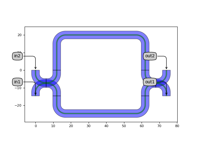
<Figure size 640x480 with 1 Axes>
Extracting the netlist
Now let’s have a look at the netlist. This is automatically extracted thanks to i3.NetlistFromLayout. IPKISS will look at the layout and check for connected ports, and generate the relevant netlist instances, terms, and connections:
nl_mzi = mzi.Netlist()

print(nl_mzi.netlist)
netlist:
--------
instances:
        - dc1 : <Single instance in netlist of PCELL_1_dc>
        - dc2 : <Single instance in netlist of PCELL_1_dc>
        - PCELL_1_wg1 : <Single instance in netlist of PCELL_1_PCELL_1_wg1>
        - PCELL_1_wg2 : <Single instance in netlist of PCELL_1_PCELL_1_wg2>

terms:
        - in1
        - in2
        - out1
        - out2

nets:
        - PCELL_1_wg1:in-dc1:out1: <OpticalLink PCELL_1_wg1:in to dc1:out1>
        - dc2:out1-out1: <OpticalLink out1 to dc2:out1>
        - dc1:in1-in1: <OpticalLink in1 to dc1:in1>
        - PCELL_1_wg1:out-dc2:in1: <OpticalLink PCELL_1_wg1:out to dc2:in1>
        - dc2:out2-out2: <OpticalLink out2 to dc2:out2>
        - dc1:in2-in2: <OpticalLink in2 to dc1:in2>
        - PCELL_1_wg2:in-dc1:out2: <OpticalLink PCELL_1_wg2:in to dc1:out2>
        - PCELL_1_wg2:out-dc2:in2: <OpticalLink PCELL_1_wg2:out to dc2:in2>
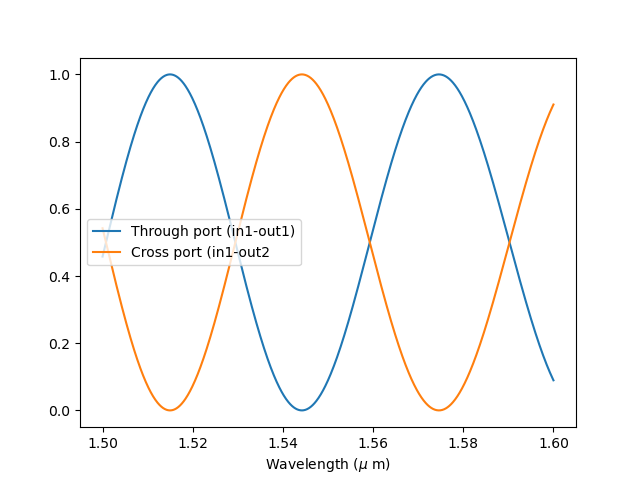
Run a simulation
Since our circuit is now equipped with a netlist, we can run a circuit simulation to see the transmission of the MZI.
import numpy as np
from pylab import plt

wavelengths = np.linspace(1.5, 1.6, 1001)

mzi_cm = mzi.CircuitModel()
S = mzi_cm.get_smatrix(wavelengths=wavelengths)

plt.plot(wavelengths, np.abs(S['out1', 'in1']) ** 2, label='Through port (in1-out1)')
plt.plot(wavelengths, np.abs(S['out2', 'in1']) ** 2, label='Cross port (in1-out2')
plt.legend()
plt.xlabel("Wavelength ($\mu$ m)")
plt.show()