PCell
PCells are the core engine in IPKISS to define parametric, re-usable cells and circuits.
i3.PCellis the base type, giving complete flexibility over the parameters and views. It is used for defining atomic devices and when you need full low-level control over layout, netlist and or model views.i3.LayoutCellcan be used to create single designs by providing a list of elements to its layout view.For composing circuits,
i3.Circuitcan be used to conveniently define circuits based on instances of other cells and a set of specifications for placement and routing.
- class ipkiss3.all.PCell(*args, **kwargs)
PCell primitive (Parametric Cell). This class is used to describe the different aspects of a component, including the layout, netlist, compact models, hierarchy etc.
A PCell has Views and Properties. It must have a name and is member of a Library.
- Parameters
- name: String that contains only ISO/IEC 8859-1 (extended ASCII py3) or pure ASCII (py2) characters
The unique name of the pcell
- class ipkiss3.all.LayoutCell(*args, **kwargs)
A PCell with an empty LayoutView,
Create a single design by instantiating i3.LayoutCell().Layout() with a list of elements.
- Parameters
- name: String that contains only ISO/IEC 8859-1 (extended ASCII py3) or pure ASCII (py2) characters
The unique name of the pcell
Notes
unit and grid attributes are there to allow for imports/exports between GDS cells defined in technologies with different metrics
Examples
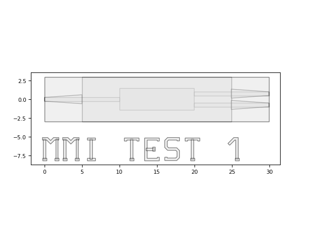
from technologies import silicon_photonics
import ipkiss3.all as i3

layer_wg = i3.Layer(0)
layer_rib = i3.Layer(1)
layer_clad = i3.Layer(2)

mmi = i3.LayoutCell(name="mmi").Layout(
    elements=[
        i3.Line(layer=layer_wg, begin_coord=(0.0, 0.0), end_coord=(10.0, 0.0), line_width=0.5),
        i3.Line(layer=layer_wg, begin_coord=(10.0, 0.0), end_coord=(19.9, 0.0), line_width=2.9),
        i3.Line(layer=layer_wg, begin_coord=(19.9, 0.75), end_coord=(29.9, 0.75), line_width=0.5),
        i3.Line(layer=layer_wg, begin_coord=(19.9, -0.75), end_coord=(29.9, -0.75), line_width=0.5),
        i3.Wedge(layer=layer_rib, begin_coord=(0.0, 0.0), end_coord=(5.0, 0.0), begin_width=0.5, end_width=1.2),
        i3.Line(layer=layer_rib, begin_coord=(5.0, 0.0), end_coord=(24.9, 0.0), line_width=6.0),
        i3.Wedge(layer=layer_rib, begin_coord=(24.9, 0.75), end_coord=(29.9, 0.75), begin_width=1.2, end_width=0.5),
        i3.Wedge(layer=layer_rib, begin_coord=(24.9, -0.75), end_coord=(29.9, -0.75), begin_width=1.2, end_width=0.5),
        i3.Line(layer=layer_clad, begin_coord=(0.0, 0.0), end_coord=(29.9, 0.0), line_width=6.0)
    ]
)

text = i3.LayoutCell(name="text").Layout(
    elements=[
        i3.PolygonText(
            layer=i3.Layer(3),
            text="MMI TEST 1",
            coordinate=(0.0, -5.0),
            alignment=(i3.TEXT.ALIGN.LEFT, i3.TEXT.ALIGN.TOP),
            font=0, height=3
        )
    ]
)

mmi_with_text = i3.LayoutCell(name="mmi_with_text").Layout(
    elements=[i3.SRef(name="mmi_ref", reference=mmi), i3.SRef(name="text_ref", reference=text)]
)
mmi_with_text.visualize()
Views
- Layout = <class 'ipkiss3.pcell.layout.layout_cell.LayoutCell.Layout'>
- class ipkiss3.all.Circuit(*args, **kwargs)
A PCell which derives its layout, netlist and model from a set of specifications in order to create a circuit.
Pre-defined instances of which the circuit is composed are specified as a dictionary insts. (This excludes connecting waveguides generated on the basis of the routing specifications).
Placement and routing is done with
i3.place_and_routeusing a combination of place_specs and route_specs (specifications as in Placement and Routing Reference).Ports are exposed using
i3.expose_portsusing port_specsThe netlist and circuit model views are derived from the layout using netlist extraction.
Create a single design by instantiating i3.Circuit directly, or create a parametric circuit by inheriting from it.
- Parameters
- exposed_ports: ( dict ), *None allowed*
Ports to be exposed, mapping {‘instance_name:port_name’: external_port_name’} map for i3.expose_ports().Set to None (default) to expose all unconnected ports
- insts: OrderedDict and key: str, value: PCell, _View
Instances of child cells which this circuit is composed of: {‘instance_name’: cell, …} where cell is an i3.PCell object.
- specs: list
Placement and routing specifications
- strict: ( bool, bool_, bool or int )
If True, any error will raise an exception and stop the program flow. If False, any routing error will give a warning and draw a straight line on an error layer. See
i3.ConnectLogicalfor more information.- name: String that contains only ISO/IEC 8859-1 (extended ASCII py3) or pure ASCII (py2) characters
The unique name of the pcell
Warning
The insts property of Circuit contains the instances specified by the user, while the instances property of the Layout view contains the full set of instances including connecting waveguides.
Notes
The following 2 are equivalent:
class MyCircuit(i3.Circuit):
    def _default_insts(self):
        return my_instances
    def _default_specs(self):
        return my_specs
    def _default_exposed_ports(self):
        return my_exposed_ports

class MyCircuit(i3.PCell)
    class Layout(i3.LayoutView):
        def _generate_instances(self, insts):
            insts += i3.place_and_route(my_instances, specs)
            return insts
        def _generate_ports(self, ports):
            ports += i3.expose_ports(self.instances, my_exposed_ports)
            return ports

    class Netlist(i3.NetlistFromLayout):
        pass

    class CircuitModel(i3.CircuitModelView):
        def _generate_model(self):
            return HierarchicalModel.from_netlistview(self.netlist_view)
Circuitprovides a convenient standardized workflow for creating specification-based layout-driven circuits. When more flexibility is needed, inherit from i3.PCell instead. Changing from i3.Circuit to i3.PCell is done as in the example above.Examples
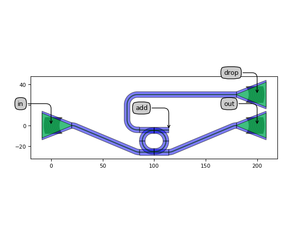
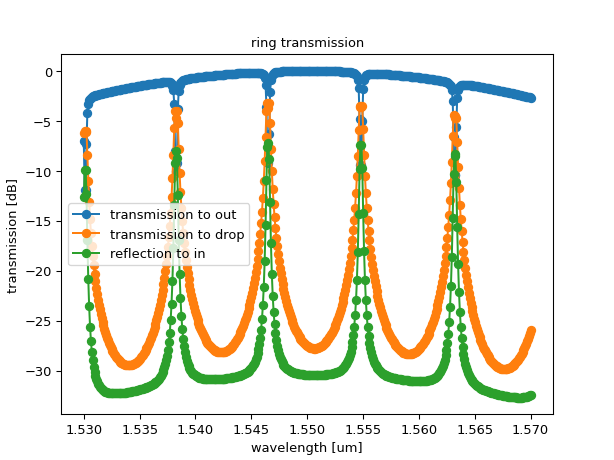
from technologies import silicon_photonics  # noqa: F401
import ipkiss3.all as i3
from picazzo3.traces.wire_wg import WireWaveguideTemplate
from picazzo3.fibcoup.curved import FiberCouplerCurvedGrating
from picazzo3.filters.ring import RingRect180DropFilter
import numpy as np
import pylab as plt

# waveguide template
waveguide_template = WireWaveguideTemplate()
waveguide_template.Layout(core_width=0.5, cladding_width=5.5)
waveguide_template.CircuitModel(n_eff=2.4, n_g=4.2)

# instances
fibcoup = FiberCouplerCurvedGrating(start_trace_template=waveguide_template)

coupler_parameters = dict(
    cross_coupling1=1j * 0.0784**0.5, straight_coupling1=0.9216**0.5, reflection_in1=1j * 0.030
)

ring = RingRect180DropFilter(
    ring_trace_template=waveguide_template, coupler_trace_templates=[waveguide_template, waveguide_template]
)
ring.Layout(bend_radius=10.0, straights=[3.0, 0.0], coupler_spacings=[0.8, 0.8])
ring.CircuitModel(coupler_parameters=[coupler_parameters, coupler_parameters])

fc_spacing = 200.0

ring_test_site = i3.Circuit(
    insts={"fc_in": fibcoup, "ring": ring, "fc_out": fibcoup, "fc_drop": fibcoup},
    specs=[
        i3.Place("fc_in:vertical_in", (0.0, 0.0)),
        i3.Place("fc_out:vertical_in", (fc_spacing, 0.0)),
        i3.FlipH("fc_out"),
        i3.Place("fc_drop:vertical_in", (fc_spacing, 30.0)),
        i3.FlipH("fc_drop"),
        i3.Place("ring", (0.5 * fc_spacing, -15.0)),
        i3.ConnectBend([("fc_in:out", "ring:in1"), ("fc_out:out", "ring:out1")], bend_radius=10),
        i3.ConnectManhattan("fc_drop:out", "ring:out2", bend_radius=10),
    ],
    exposed_ports={
        "fc_in:vertical_in": "in",
        "fc_out:vertical_in": "out",
        "fc_drop:vertical_in": "drop",
        "ring:in2": "add",
    },
)

ring_test_layout = ring_test_site.Layout()
ring_test_layout.visualize(annotate=True)

sim_wavelengths = np.linspace(1.53, 1.57, 500)
ring_test_cm = ring_test_site.CircuitModel()

ring_test_S = ring_test_cm.get_smatrix(sim_wavelengths)
plt.figure()
plt.title("ring transmission")
plt.xlabel("wavelength [um]")
plt.ylabel("transmission [dB]")
plt.plot(
    sim_wavelengths, 10 * np.log10(np.abs(ring_test_S["out", "in"]) ** 2), "o-", label="transmission to out"
)
plt.plot(
    sim_wavelengths, 10 * np.log10(np.abs(ring_test_S["drop", "in"]) ** 2), "o-", label="transmission to drop"
)
plt.plot(sim_wavelengths, 10 * np.log10(np.abs(ring_test_S["in", "in"]) ** 2), "o-", label="reflection to in")
plt.legend()
plt.show()
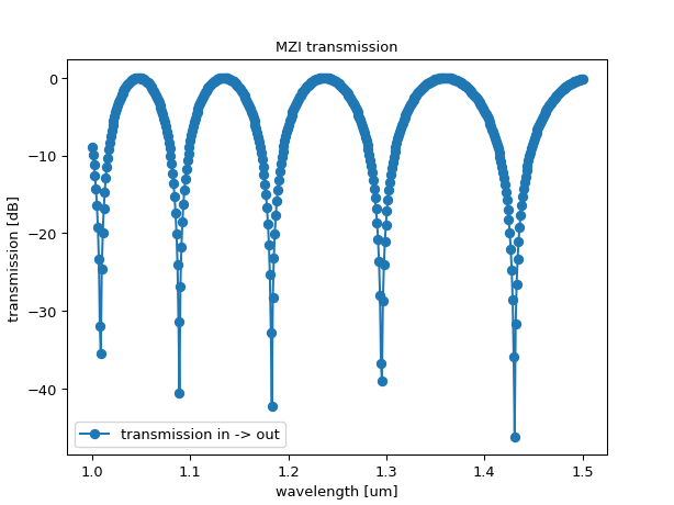
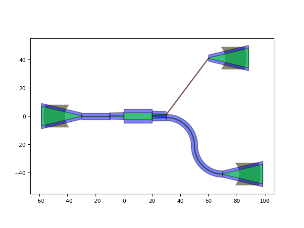
from technologies import silicon_photonics  # noqa: F401
import ipkiss3.all as i3
from picazzo3.traces.wire_wg import WireWaveguideTemplate
import numpy as np
import matplotlib.pyplot as plt
from picazzo3.wg.splitters import WgYSplitter, WgYCombiner

# waveguide templates for MZI arms
wg_t_arm1 = WireWaveguideTemplate()
wg_t_arm1.Layout(core_width=1.0, cladding_width=5.5)
wg_t_arm1.CircuitModel(n_eff=3.2, n_g=3.9)

wg_t_arm2 = WireWaveguideTemplate()
wg_t_arm2.Layout(core_width=0.5, cladding_width=5.5)
wg_t_arm2.CircuitModel(n_eff=2.4, n_g=4.15)

mzi = i3.Circuit(
    insts={"splitter": WgYSplitter(), "combiner": WgYCombiner()},
    specs=[
        i3.Place("splitter", (0, 0)),
        i3.PlaceRelative("combiner", "splitter", (50, 0)),
        i3.ConnectManhattan("splitter:arm1", "combiner:arm1", "arm1", trace_template=wg_t_arm1),
        i3.ConnectManhattan("splitter:arm2", "combiner:arm2", "arm2", trace_template=wg_t_arm2),
    ],
    exposed_ports={
        "splitter:center": "in",
        "combiner:center": "out",
    },
)

mzi_layout = mzi.Layout()
mzi_layout.visualize(annotate=True)
sim_wavelengths = np.linspace(1.0, 1.5, 500)
mzi_cm = mzi.CircuitModel()

mzi_test_S = mzi_cm.get_smatrix(sim_wavelengths)
plt.figure()
plt.title("MZI transmission")
plt.xlabel("wavelength [um]")
plt.ylabel("transmission [dB]")
plt.plot(
    sim_wavelengths, 10 * np.log10(np.abs(mzi_test_S["out", "in"]) ** 2), "o-", label="transmission in -> out"
)
plt.legend()
plt.show()
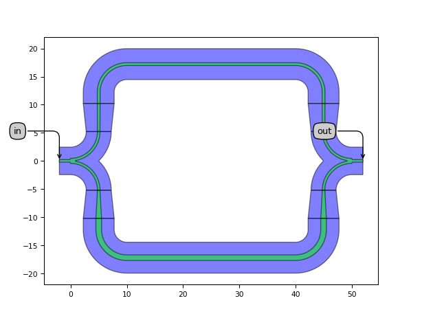
from technologies import silicon_photonics  # noqa: F401
from ipkiss3 import all as i3

from picazzo3.fibcoup.curved import FiberCouplerCurvedGrating
from picazzo3.filters.mmi.cell import MMI1x2Tapered
from picazzo3.traces.wire_wg.trace import WireWaveguideTemplate

# Create the template for the MMI
mmi_trace_template = WireWaveguideTemplate()
mmi_trace_template.Layout(core_width=5.0, cladding_width=10.0)

mmi_access_template = WireWaveguideTemplate()
mmi_access_template.Layout(core_width=1.0, cladding_width=5.0)

mmi = MMI1x2Tapered(
    mmi_trace_template=mmi_trace_template,
    input_trace_template=mmi_access_template,
    output_trace_template=mmi_access_template,
    trace_template=i3.TECH.PCELLS.WG.DEFAULT,
)
mmi.Layout(transition_length=10.0, length=20.0, trace_spacing=2.0)

# Create the template for the grating couplers
end_wg_tmpl = WireWaveguideTemplate()
end_wg_tmpl.Layout(core_width=10.0, cladding_width=2 * i3.TECH.WG.TRENCH_WIDTH + 10.0)

coupler = FiberCouplerCurvedGrating(
    start_trace_template=i3.TECH.PCELLS.WG.DEFAULT, wide_trace_template=end_wg_tmpl
)
coupler.Layout(period_x=1.0, focal_distance_x=20.0)

# Place and route the MMI and grating couplers
circuit = i3.Circuit(
    insts={"coupler_in": coupler, "coupler_out1": coupler, "coupler_out2": coupler, "mmi": mmi},
    specs=[
        i3.Place("mmi", (0, 0)),
        i3.PlaceRelative("coupler_in", "mmi", (-50, 0)),
        i3.PlaceRelative("coupler_out1:out", "mmi:out1", (40, -40)),
        # Place ports too close together for bend_radius=20:
        i3.PlaceRelative("coupler_out2:out", "mmi:out2", (30, 40)),
        i3.FlipH(["coupler_out1", "coupler_out2"]),
        i3.ConnectBend(
            [("coupler_in:out", "mmi:in"), ("mmi:out1", "coupler_out1:out"), ("mmi:out2", "coupler_out2:out")],
            bend_radius=20,
        ),
    ],
    strict=False,  # Will draw a straight line on an error layer
)
lv = circuit.get_default_view(i3.LayoutView)
lv.visualize()
i3.place_and_route and i3.Circuit can be used to place and route electrical components as well.:
def __example4(self):
    """An important requirement when using i3.Circuit and i3.place_and_route is that the
    ports should have an angle.
    For optical ports, this will always be the case. For electrical ports, however,
    the port is not always specified.

    In this example, we'll extend ElectricalWire and Picazzo's PhaseModulator to specify the
    angles on its electrical ports.

    """
    from technologies import silicon_photonics  # noqa: F401
    import ipkiss3.all as i3
    from picazzo3.modulators.phase import PhaseModulator as _PhaseModulator

    class ElectricalWire(i3.ElectricalWire):
        class Layout(i3.ElectricalWire.Layout):
            def _generate_ports(self, ports):
                ports = super(ElectricalWire.Layout, self)._generate_ports(ports)
                angles = self.shape.angles_deg()
                in_angle, out_angle = angles[0] + 180, angles[-1]
                ports["in"].angle = in_angle
                ports["out"].angle = out_angle
                return ports

    class PhaseModulator(_PhaseModulator):
        class Layout(_PhaseModulator.Layout):
            def _generate_ports(self, ports):
                ports = super(PhaseModulator.Layout, self)._generate_ports(ports)
                ports["electrical0"].angle = 90
                ports["electrical1"].angle = -90
                return ports

    wire = ElectricalWire()
    phmod = PhaseModulator()
    phmod.Layout(length=20)

    circuit = i3.Circuit(
        insts={"wire": wire, "modulator": phmod},
        specs=[
            i3.Place("modulator:out", (0, 0)),
            i3.Place("wire:in", (0, 30)),
            i3.ConnectManhattan("modulator:electrical0", "wire:in"),
        ],
        exposed_ports={
            "wire:out": "out0",
            "modulator:out": "out1",
            "modulator:in": "out1",
        },
    )

    lay = circuit.Layout()
    lay.visualize(annotate=True)
Views
- Layout = <class 'ipkiss3.pcell.circuit.Circuit.Layout'>
- Netlist = <class 'ipkiss3.pcell.circuit.Circuit.Netlist'>
- CircuitModel = <class 'ipkiss3.pcell.circuit.Circuit.CircuitModel'>