Note
Click here to download the full example code
Simulating an aperture with CAMFR
This simple example illustrates the integration of SlabSim in IPKISS. It requires the IPKISS AWG Designer module. We make a simple aperture and run a CAMFR simulation on it.
Note: do not use this aperture in a real design, this is only for illustration purposes and not designed optimally.
Getting started
We start by importing the technology with other required modules:
from technologies import silicon_photonics  # noqa: F401
from ipkiss3 import all as i3
import numpy
import pylab as plt
From IPKISS’ AWG Designer, we import the following:
from awg_designer.all import OpenTransitionAperture, SimpleSlabMode, SlabTemplate
from picazzo3.traces.rib_wg import RibWaveguideTemplate
The Environment object is needed to specify the wavelength of interest.
from pysics.basics.environment import Environment
Template for the free propagation region. This defines the layers, slab modes, etc.
slab_t = SlabTemplate()
slab_t.Layout(slab_layers=[i3.PPLayer(i3.TECH.PROCESS.WG, i3.TECH.PURPOSE.DF_AREA)])
slab_t.SlabModes(modes=[SimpleSlabMode(name="TE0", n_eff=2.8, n_g=3.2, polarization="TE")])
<SlabTemplate.SlabModes view 'TEMPLATE_1:slabmodes'>
Specify the wavelength of interest
environment = Environment(wavelength=1.55)
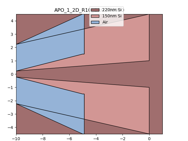
The aperture
Make an aperture consisting of a transition between two trace templates. Trace template at the aperture
ap_wg_t = RibWaveguideTemplate()
ap_wg_t.Layout(core_width=2.0)
<RibWaveguideTemplate.Layout view 'RIB_WG_TEMPLATE_1:layout'>
Trace template at the waveguide port
wg_t = i3.TECH.PCELLS.WG.DEFAULT
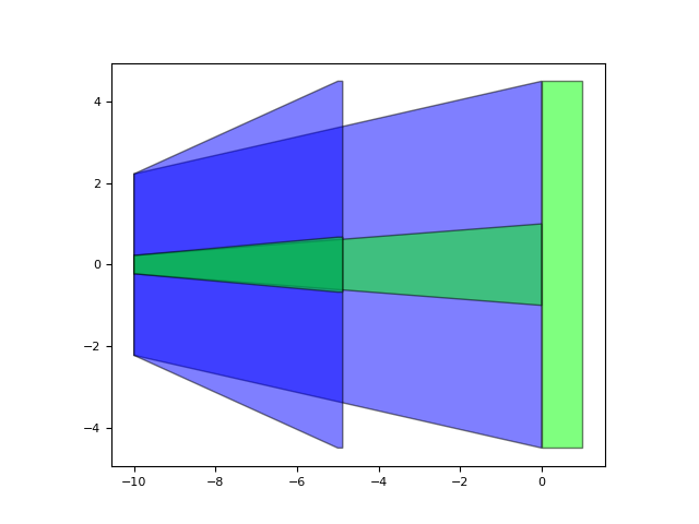
The aperture
ap = OpenTransitionAperture(slab_template=slab_t, aperture_trace_template=ap_wg_t, trace_template=wg_t)
ap_lo = ap.Layout()  # the length is calculated by default
ap_lo.visualize()
ap_lo.visualize_2d()
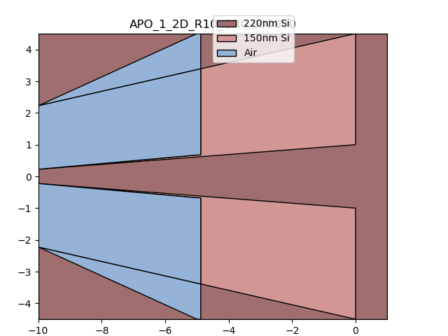
<Figure size 640x480 with 1 Axes>
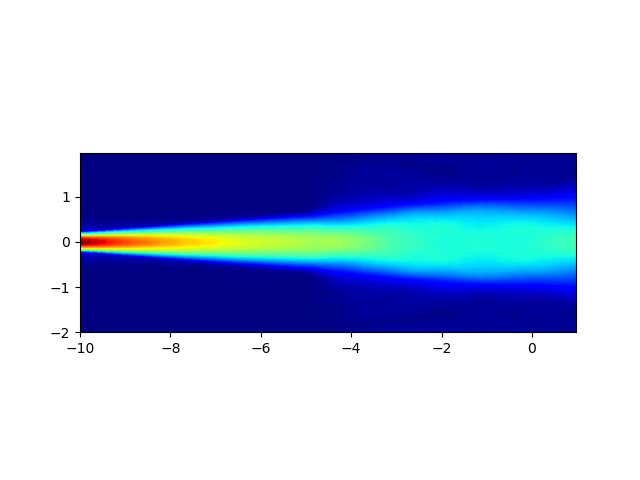
Get the field profile at the aperture
This will execute a CAMFR simulation. By putting verbose=True, the simulation prints the wavelength and effective indices used for the simulation.
ap_sm = ap.FieldModelFromCamfr()
f = ap_sm.get_fields(environment=environment, verbose=True)
f.visualize()
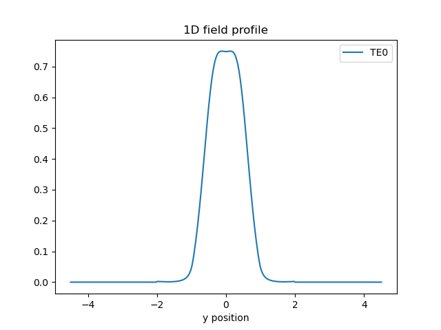
Running camfr simulation:
* Device: <OpenTransitionAperture.Layout view 'APO_1:layout'>
* Wavelength = 1.55 um
* Effective indices used:
  - 220nm Si: 2.823028436355695
  - 150nm Si: 2.5026463677413866
  - Air: 1.0

<Figure size 640x480 with 1 Axes>
Show the far field
ff = ap_sm.get_far_field(environment=environment)
ff.visualize()
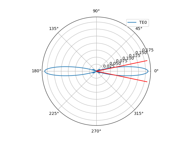
<Figure size 640x480 with 1 Axes>
Plot the full field inside the waveguide aperture:
f2d = ap_sm.get_aperture_fields2d(environment=environment)
f2d.visualize()
<Figure size 640x480 with 1 Axes>
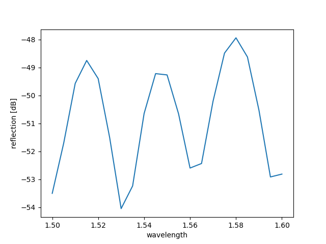
CircuitModel: Check the backreflection of the aperture
The circuitmodel will get this directly from the CAMFR simulation
ap_cm = ap.CircuitModel()
wavelengths = numpy.linspace(1.5, 1.6, 21)
s_matrix = ap_cm.get_smatrix(wavelengths=wavelengths)
refl_aperture = 20.0 * numpy.log10(numpy.abs(s_matrix["in", "in"]))
Plot the reflection of the aperture. You can see some oscillations which are fabry-perot resonances caused by reflections due to the discontinuities along the profile of the aperture.
plt.plot(wavelengths, refl_aperture)
plt.xlabel("wavelength")
plt.ylabel("reflection [dB]")
plt.show()
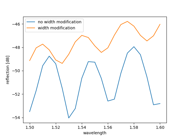
By increasing wire_end_width, we expect that there is less reflection from the discontinuity between deep and shallow etch. By adjusting this value, the intensity of the Fabry-Perot resonance should decrease.
ap_lo.transition_parameters = {"wire_end_width": 3.0}
ap_lo.visualize_2d()
<Figure size 640x480 with 1 Axes>
s_matrix = ap_cm.get_smatrix(wavelengths=wavelengths)
refl_aperture_new = 20.0 * numpy.log10(numpy.abs(s_matrix["in", "in"]))
plt.plot(wavelengths, refl_aperture, label="no width modification")
plt.plot(wavelengths, refl_aperture_new, label="width modification")
plt.xlabel("wavelength")
plt.ylabel("reflection [dB]")
plt.legend()
plt.show()
Total running time of the script: ( 6 minutes 26.333 seconds)