Layout: basics
In this tutorial we’ll guide you through the basics of creating a layout in IPKISS. We start with drawing simple waveguides, then learn how to create a simple PCell, and then draw a circuit consisting of several PCells and waveguides. Finally we explain how to parametrize this cell and run a basic netlist extraction and circuit simulation.
Drawing waveguides
When designing a Photonic Integrated Circuit (PIC), you’ll be using waveguides most of the time. So let’s draw a simple waveguide in IPKISS to get started.
Note
If you want to draw a device using simple primitive elements such as rectangles, circles, wedges and so on, you can have a look at elements and layers and shapes.
First, please open a new file in your favorite code editor. If you haven’t installed one yet, we recommend you follow the PyCharm (tutorial) to get started. Feel free to use another editor if you’re comfortable with writing Python code already.
Now write the following code in the new file:
# First we load a PDK (demolib in this case)
import demolib.all as demo
import ipkiss3.all as i3
Let’s explain what we did: we started off with importing a demo PDK called demolib.
demolib is located in your samples folder (windows: %USERPROFILE%\luceda\samples\ipkiss390, linux: ~/luceda/samples/ipkiss390),
under demo/libraries/demolib/ipkiss. Make sure this folder is in your PYTHONPATH.
If you loaded the samples project this
should be already the case.
Then we import ipkiss3.all, and assign it to the name i3 (like a shorthand notation). ipkiss3.all is a
namespace which contains a series of useful classes and functions which we’ll use throughout this tutorial.
Next, let’s define a waveguide template. A waveguide template describes the properties of the waveguide such as waveguide layers and widths, and model parameters.
wg_t = demo.SiWireWaveguideTemplate()
wg_t_lo = wg_t.Layout(core_width=0.5)
wg_t_cm = wg_t.CircuitModel(n_eff=2.4, n_g=4.3, center_wavelength=1.55)
Notice we’ve selected the wire waveguide template from the demo PDK.
You can also choose demo.SiRibWaveguideTemplate if you want a shallow-etched waveguide.
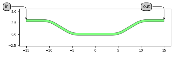
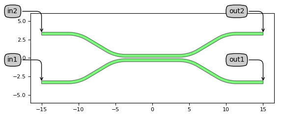
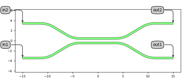
A waveguide is now drawn using this waveguide template, and with a given shape:
# Define a rounded waveguide
wg = i3.RoundedWaveguide(name='MyWaveguide', trace_template=wg_t)
wg_lo = wg.Layout(shape=[(-15, 3), (-10, 3), (-5, 0), (5, 0), (10, 3), (15, 3)])
Finally let’s visualize this waveguide:
wg_lo.visualize(annotate=True)
When you execute this Python script, a window will pop up displaying the visualized cell:
You can download the full example: demolib_waveguide.py.
Waveguides and waveguide templates are explained in more detail in waveguide templates. This is not required to continue this tutorial.
Creating a PCell
When drawing a layout mask you will typically create a library of basic devices. Those devices are then combined to make larger devices or circuits. The basic element of reuse is called a PCell. To illustrate this concept let’s create a directional coupler PCell using two waveguides.
First, create a new file, and type the following:
# First we load a PDK (demolib in this case)
import demolib.all as demo
import ipkiss3.all as i3
Next, as we’ve done previously let’s define our waveguide template so IPKISS knows how to draw the waveguides:
# import [...]

wg_t = demo.SiWireWaveguideTemplate()
wg_t_lo = wg_t.Layout(core_width=0.5)

# PCell code [...]
Next we build the directional coupler PCell. A PCell in IPKISS is defined using i3.PCell.
We add a i3.LayoutView which holds all layout information:
class DirectionalCoupler(i3.PCell):
    class Layout(i3.LayoutView):
        def _generate_instances(self, insts):
           # code to draw waveguides goes here
           return insts
Note that we’ve also defined the _generate_instances function. This is where we’ll draw our waveguides.
We’ll put in the same waveguide as we’ve drawn in the previous step of the tutorial, except we change the name.
We always need to give a meaningful name to the cell, as that’s the name that is going to be written to GDS.
In this case we use the parent cell’s name (self.name) and we add the _wg suffix.
An i3.SRef (‘scalar reference’) is used to place the waveguide
inside the DirectionalCoupler PCell.
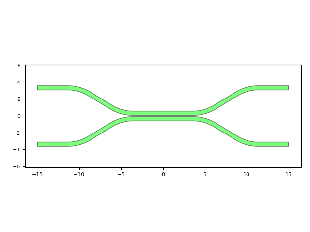
Here’s how the code inside _generate_instances looks like now:
class DirectionalCoupler(i3.PCell):
    class Layout(i3.LayoutView):
        def _generate_instances(self, insts):

            wg = i3.RoundedWaveguide(name=self.name + '_wg', trace_template=wg_t)
            wg.Layout(shape=[(-15, 3), (-10, 3), (-5, 0), (5, 0), (10, 3), (15, 3)])

            insts += i3.SRef(name='wg_top', reference=wg)
            return insts
To finish the directional coupler, we need to add a second waveguide, which is a mirrorred version of the first waveguide.
We also need to move the top waveguide a bit up, and the bottom waveguide a bit down, so we get a desired gap between them.
That vertical distance is calculated as 0.5 * core_width + 0.5 * gap, so we can define the two instances as follows:
insts += i3.SRef(name='wg_top', reference=wg, position=(0, 0.5 * core_width + 0.5 * gap))
insts += i3.SRef(name='wg_bottom', reference=wg, position=(0, -0.5 * core_width - 0.5 * gap), transformation=i3.VMirror())
The final code for our directional coupler now looks like this:
# First we load a PDK (demo PDK in this case)
import demolib.all as demo
import ipkiss3.all as i3

# Create a waveguide template (contains cross-sectional information)
wg_t = demo.SiWireWaveguideTemplate()
wg_t_lo = wg_t.Layout(core_width=0.5)

class DirectionalCoupler(i3.PCell):
    class Layout(i3.LayoutView):
        def _generate_instances(self, insts):
            # Define some parameters
            gap = 0.2
            core_width = wg_t_lo.core_width


            # Define a rounded waveguide
            wg = i3.RoundedWaveguide(name=self.name+'_wg1', trace_template=wg_t)
            wg.Layout(shape=[(-15, 3), (-10, 3), (-5, 0), (5, 0), (10, 3), (15, 3)])

            # Define instances
            insts += i3.SRef(name='wg_top', reference=wg, position=(0, 0.5 * core_width + 0.5 * gap))
            insts += i3.SRef(name='wg_bottom', reference=wg, position=(0, -0.5 * core_width - 0.5 * gap), transformation=i3.VMirror())
            return insts
We can also visualize this directional coupler by adding the following code to the bottom of the python file, and then executing the file:
dc = DirectionalCoupler()
dc_lay = dc.Layout()
dc_lay.visualize()
Also, this layout can be written to GDSII. To do so, you can use the write_gdsii function:
dc_lay.write_gdsii('dircoup.gds')
This will create a file called dircoup.gds in the same folder as where you executed the script.
Finally let’s add optical ports to this device. The ports contain information such as the position, angle, which
trace template is attached to them and so on. It is used to interface this device with the outside world.
Normally we can use i3.OpticalPort to define them, but in this case we can
copy them from the existing ports in the waveguide instances.
For that we use the function i3.expose_ports:
class DirectionalCoupler(i3.PCell):
    class Layout(i3.LayoutView):
        def _generate_ports(self, ports):
            return i3.expose_ports(self.instances,
                                          {'wg_bottom:in': 'in1',
                                           'wg_top:in': 'in2',
                                           'wg_bottom:out': 'out1',
                                           'wg_top:out': 'out2'})
As you can see we remap the port names. For example, the in port of the bottom waveguide is copied,
and then renamed to in1. Ok, let’s visualize the directional coupler again. This time, we add the
annotate=True argument to the visualization function, so it also displays the ports:
dc = DirectionalCoupler()
dc_lay = dc.Layout()
dc_lay.visualize(annotate=True)
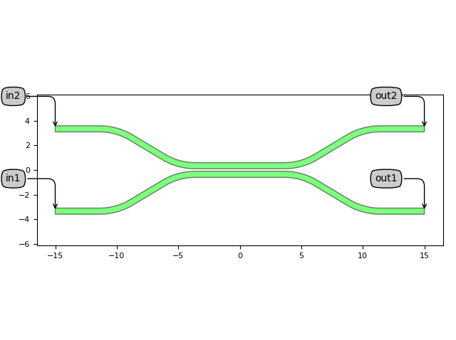
The full examples can be downloaded: demolib_dircoup.py.
Note
If you want to learn more about the concepts of PCells, Layout views, which drawing primitives are available and so on, please visit the layout guide. For reference material please visit layout reference. This is not strictly required to continue this tutorial.
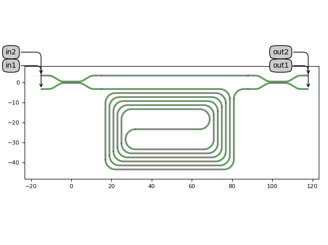
Building a small circuit
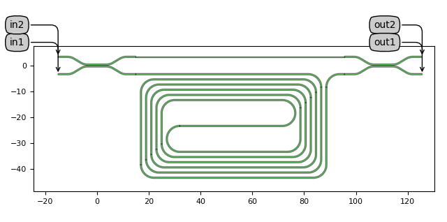
As next step, we’ll build a Mach-Zehnder Interferometer (MZI) using the directional coupler that we juist built. We’ll add a spiral in one of the waveguide arms to make a long delay line.

|
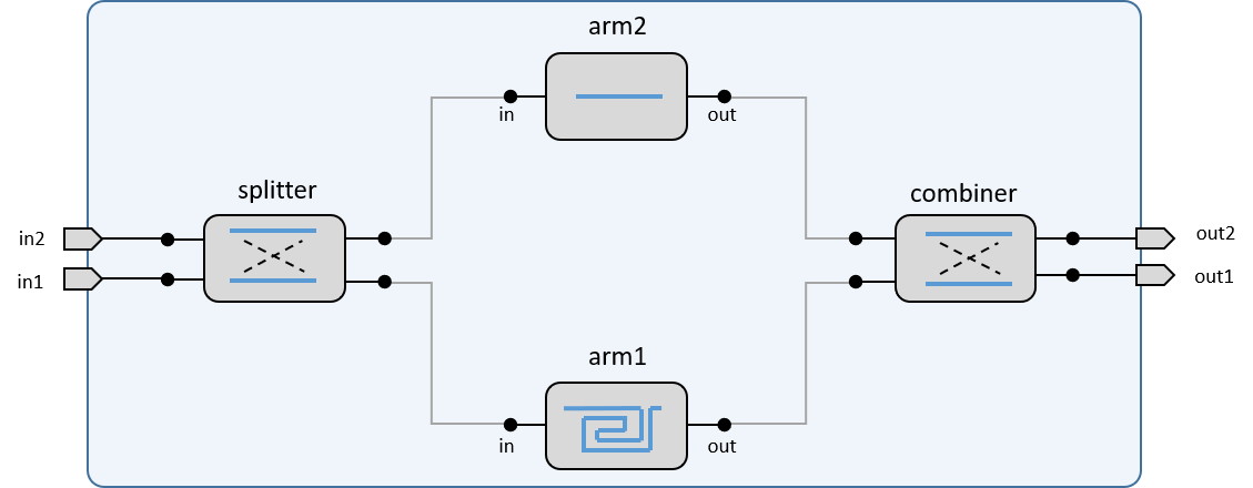
|
Building blocks used to create MZI |
MZI schematic |
To start, add the following code at the bottom of the file we just created:
# ...
from picazzo3.wg.spirals import FixedLengthSpiralRounded

class MZI(i3.PCell):
    class Layout(i3.LayoutView):

        def _generate_instances(self, insts):

            dc = DirectionalCoupler()

            spiral = FixedLengthSpiralRounded(name=self.name + "_SPIRAL",
                                              trace_template=wg_t, n_o_loops=3, total_length=1000)
            spiral_lo = spiral.Layout()

            ...
The length of the waveguide should be as long as the distance between the in and output port of the spiral,
which can be calculated using spiral_lo.ports['out'].position.x - spiral_lo.ports['in'].position.x.
With these cells instantiated, we can now call i3.place_and_route,
which is the main workhorse for layout placement and routing:
i3.place_and_route(
    insts={
        'splitter': dc,
        'combiner': dc,
        'arm1': spiral,
    },
    specs=[
        # Placement:
        i3.Place('splitter', (0, 0)),
        i3.Join([
            ('splitter:out1', 'arm1:in'),
            ('combiner:in1', 'arm1:out'),
        ]),
        i3.FlipV('arm1'),

        # Routing:
        i3.ConnectManhattan('splitter:out2', 'combiner:out2'),
    ],
    strict=False
)
What you can see here is that we define a set of rules for the device placement. In this specific case we used
i3.Place: to place a device at a certain location (optionally, you can select a port, and define angles),
i3.Join: to join two ports head to tail (you can also specify a list of multple joins, as was done in the example),
i3.FlipV: to flip a component vertically.
For the routing we specify a Manhattan connection between port ‘out2’ of the splitter and port ‘out2’ of the combiner:
i3.ConnectManhattan: to create a manhattan waveguide between the specified ports
Some small remarks on the placement and routing:
For the Join spec, we connected the 2 directional couplers with the delay line with only 2 joins.
When we mirror the spiral using FlipV, what we’re saying is that during the placement, we want a vertically flipped version of the spiral to be placed. The spiral is mirrored around it’s own local y=0 axis.
The ConnectManhattan spec results in a straight waveguide between the specified (already placed) ports. Note that if the specified ports would not be on the same height then the connector would not create a straight waveguide and the delay length would no longer be correct.
verify: optionally you can set the verify argument (by default, it equals True). The verify function checks whether the inputs to the function are correct, and after placement checks whether the placement specifications are not contradicting each other.
strict: optionally you can also set the strict argument (by default, it equals True). If True, any connector error will raise an exception and stop the program flow. If False, any connector error will give a warning, and draw a straight line on an error layer.
Please check the placement and routing reference and the connector reference to learn about all possible specifications that you can use to define your circuit.
The final code is now this:
from picazzo3.wg.spirals import FixedLengthSpiralRounded

class MZI(i3.PCell):
    class Layout(i3.LayoutView):
        def _generate_instances(self, insts):

            spiral = FixedLengthSpiralRounded(name=self.name + "_SPIRAL",
                                              trace_template=wg_t, n_o_loops=3, total_length=1000)
            spiral_lo = spiral.Layout()

            insts += i3.place_and_route(
                insts={
                    'splitter': dc,
                    'combiner': dc,
                    'arm1': spiral,
                },
                specs=[
                    i3.Place('splitter', (0, 0)),
                    i3.Join([
                        ('splitter:out1', 'arm1:in'),
                        ('combiner:in1', 'arm1:out'),
                    ]),
                    i3.FlipV('arm1'),
                    i3.ConnectManhattan('splitter:out2', 'combiner:out2'),
                ]
            )
            return insts

        def _generate_ports(self, ports):
            return i3.expose_ports(self.instances,
                                   {'splitter:in1': 'in1',
                                    'splitter:in2': 'in2',
                                    'combiner:out1': 'out1',
                                    'combiner:out2': 'out2'})

mzi = MZI()
mzi_lo = mzi.Layout()
mzi_lo.visualize(annotate=True)
And our MZI is ready. If you want you can export this to a GDSII file (mzi_lo.write_gdsii('mzi.gds'))
and inspect it with a GDSII viewer.
Note
You can still place individual SRef elements using the method described in the directional coupler, but place_and_route does a lot of the work of calculating positions, angles and transformations for you, so that you don’t have to do them yourself.
Ignore errors in specs
As we quickly mentioned earlier, the place_and_route method has a verify argument.
To check how it works, let’s put an additional spec: i3.Place('combiner', (0, -20)). If you then run
the script again, you’ll get this error:
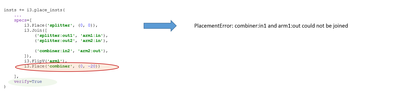
Sometimes it’s difficult to tell from the error what is going wrong.
That’s because when 2 specs are contradicting it’s very difficult to know which is the one the user actually wanted in the first place.
If you still want to try and place the layout (being aware that it won’t give a valid layout), you can put verify=False and rerun:
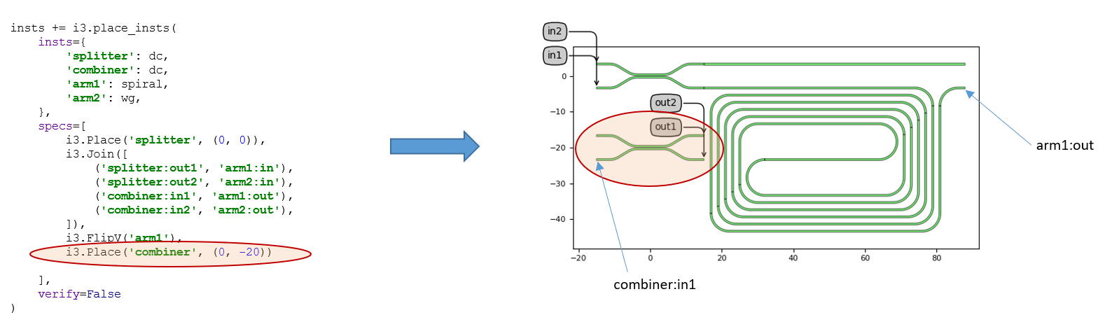
Here you can see that we Place the combiner at location (0, -20), but a Join spec was also defined
which would connect the combiner to arm1 (the spiral). That is impossible, hence the error that was raised.
Parametrize cell and reuse
One very powerful concept in design automation is parametrized cells. For example, in the MZI we created above, there’s several things we’d might want to change:
Change the spiral length.
Use a different waveguide width throughout the whole circuit.
Use a different directional coupler (perhaps one from a PDK, or one from the picazzo library).
In this part we’ll learn you how to parametrize all of these aspects. In the end you’ll have created a PCell that can be used in a variety of situations. In addition, the file can be easily added to a user library, so that you and your colleagues can reuse the component.
Parametrize spiral length
Let’s make the spiral length a parameter of the MZI. To do this we need to make a small change to our PCell as highlighted below:
class MZI(i3.PCell):
    spiral_length = i3.PositiveNumberProperty(doc="Length of the spiral in the MZI", default=1000)

    class Layout(i3.LayoutView):

        def _generate_instances(self, insts):
            dc = DirectionalCoupler()

            spiral = FixedLengthSpiralRounded(name=self.name + "_SPIRAL",
                                              trace_template=wg_t, n_o_loops=3, total_length=self.spiral_length)
            spiral_lo = spiral.Layout()
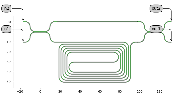
Now, when we instantiate the MZI we can choose the spiral_length parameter:
mzi = MZI(spiral_length=1100)
mzi_lo = mzi.Layout()
mzi_lo.visualize(annotate=True)
The full file can be downloaded: demolib_mzi.py (note: it also contains all other parametrizations
that we talk about below).
Note
Setting parameters on the PCell or Layout level? It’s possible to set parameters either on the pcell or on the layout level. As a rule of thumb, it’s better to move the parameters to the most specific view where they are relevant. A layout parameter belongs in the Layout view, a simulation parameter belongs to the CircuitModel view. Design parameters that are crucial to the device operation are usually placed on the PCell level. As the spiral length is a design parameter, we’ll put it on the PCell level.
Parametrizing the trace template
In many devices and circuits, trace_template is a parameter. It’s used to describe how waveguides
(which are basically optical traces) are generated (template). Let’s first parametrize the trace_template in
the directional coupler (and while we’re at it, let’s also parametrize the gap):
class DirectionalCoupler(i3.PCell):
    trace_template = i3.TraceTemplateProperty(doc="Waveguide template used for creating the waveguides.")

    class Layout(i3.LayoutView):
        gap = i3.PositiveNumberProperty(default=0.2, doc="Gap between the two waveguides")

        def _generate_instances(self, insts):
            gap = self.gap
            core_width = self.trace_template.core_width

            # Define a rounded waveguide
            wg = i3.RoundedWaveguide(name=self.name + '_wg1', trace_template=self.trace_template)
            wg.Layout(shape=[(-15, 3), (-10, 3), (-5, 0), (5, 0), (10, 3), (15, 3)])

            # Define instances
            insts += i3.SRef(name='wg_top', reference=wg, position=(0, 0.5 * (core_width + gap)))
            insts += i3.SRef(name='wg_bottom', reference=wg, position=(0, -0.5 * (core_width + gap)),
                             transformation=i3.VMirror())
            return insts
As you can see, the waveguide is now created using the trace_template property from the directional coupler PCell.
We can use it to create directional couplers with different waveguide templates:
# Create a waveguide template with core width = 0.4 um
wg_t = demo.SiWireWaveguideTemplate()
wg_t_lo = wg_t.Layout(core_width=0.4)


dc = DirectionalCoupler(trace_template=wg_t)
dc_lay = dc.Layout(gap=0.2)
dc_lay.write_gdsii('dircoup2a.gds')
dc_lay.visualize(annotate=True)

# Create a waveguide template with core width = 0.8 um
wg_t2 = demo.SiWireWaveguideTemplate()
wg_t2_lo = wg_t2.Layout(core_width=0.9)


dc = DirectionalCoupler(trace_template=wg_t)
dc_lay = dc.Layout(gap=0.5)
dc_lay.write_gdsii('dircoup2b.gds')
dc_lay.visualize(annotate=True)
|
|
|
|
The same parametrization can happen to the MZI:
class MZI(i3.PCell):
    trace_template = i3.TraceTemplateProperty()
    spiral_length = i3.PositiveNumberProperty(doc="Length of the spiral in the MZI", default=1000)

    class Layout(i3.LayoutView):

        def _generate_instances(self, insts):
            wg_t = self.trace_template

            spiral = FixedLengthSpiralRounded(trace_template=wg_t,
                                              n_o_loops=3,
                                              total_length=self.spiral_length)
            spiral_lo = spiral.Layout()

            # [...]
Note: at this point, the trace template of the directional coupler and the trace template of the spiral may have a different core width, as we’ve only updated the trace_template of the spiral, and we’re still using the original directional coupler. In order to make the PCell fully consistent we should make sure the same trace template is also used in the directional coupler. We will solve this in the next section by parametrizing the directional coupler and providing a good default value.
Parametrizing the directional coupler
Finally, let’s assume you want to change the directional coupler (DC) that’s being used in the MZI. Maybe you want to set an imbalance (i.e., no perfect 50-50 coupling) by changing the gap or coupler length, reuse a validated directional coupler from a PDK, or use one from the picazzo library, which is Luceda’s generic component library. To do so, we add a new property to the MZI class:
class MZI(i3.PCell):
    trace_template = i3.TraceTemplateProperty()
    spiral_length = i3.PositiveNumberProperty(doc="Length of the spiral in the MZI", default=1000)

    dc = i3.ChildCellProperty()

    def _default_dc(self):
        dc = DirectionalCoupler(name=self.name + "_DC",
                                trace_template=self.trace_template)
        return dc

    class Layout(i3.LayoutView):

        def _generate_instances(self, insts):
            dc = self.dc
            wg_t = self.trace_template

            # [...]
As you can see in the code above, we defined the directional coupler using
a i3.ChildCellProperty.
We can also provide a default value, which is the one which will be used when no dc parameter is passed when
creating the MZI. Note that we are hierarchically passing on the trace_template. This is very useful:
we only need to define the trace_template on the MZI, and the MZI will automatically create directional couplers
with the correct trace templates.
Now, we can either
instantiate the MZI with default parameters (in which the
_default_dcfunction will be called)or we can instantiate it and pass on a new directional coupler from picazzo
Here’s how it works:
# Create the waveguide template
wg_t = demo.SiWireWaveguideTemplate()
wg_t_lo = wg_t.Layout(core_width=0.5)

# Option 1: use default value for the directional coupler
mzi = MZI(trace_template=wg_t)
mzi_lo = mzi.Layout(name='MZI_SP1100_WG500', spiral_length=1100)
mzi_lo.visualize(annotate=True)

# Option 2: use a directional coupler from picazzo
from picazzo3.wg.dircoup import SBendDirectionalCoupler
dc = SBendDirectionalCoupler(trace_template1=wg_t)
dc.Layout(bend_radius=5, coupler_length=10)
mzi = MZI(trace_template=wg_t, dc=dc)
mzi_lo = mzi.Layout(name='MZI_SP1100_R10_WG500', spiral_length=1100)
mzi_lo.visualize(annotate=True)
|
|
# Option 1: Use default value for the directional coupler
mzi = MZI(trace_template=wg_t)
|
# Option 2: use a directional coupler from picazzo
dc = SBendDirectionalCoupler(trace_template=wg_t)
dc.Layout(bend_radius=5, coupler_length=10)
mzi = MZI(trace_template=wg_t, dc=dc)
|
Final code for the parametrized MZI for download: demolib_mzi2.py.
Verifying your layout
There are several ways you can verify your layout. Except for a thorough layout Design Rule Check (DRC), which is usually something you want to do before tape-out, there’s other ways you can verify the layout during design:
Netlist extraction: you can extract the netlist from layout to check if the connectivity is as expected.
Post-layout simulation: you can run a circuit simulation to check the device behavior.
Netlist extraction
To run optical netlist extraction you need to add a netlist view to your layout. We use
i3.NetlistFromLayout, which can extract the optical netlist based on
the layout information defined in the LayoutView.
class MZI(i3.PCell):
    # ...
    class Netlist(i3.NetlistFromLayout):
        pass
Netlist extraction assumes that each cell placed in the layout also has a NetlistView. Since we haven’t defined a NetlistView for our directional coupler yet, let’s just take the directional coupler from the picazzo library, instantiate it, and create a new MZI using this directional coupler.
# Create the waveguide template
wg_t = demo.SiWireWaveguideTemplate()
wg_t_lo = wg_t.Layout(core_width=0.5)

# Use directional coupler from picazzo
dc = SBendDirectionalCoupler(name="SBendDC", trace_template1=wg_t)
dc.Layout(bend_radius=5, coupler_length=10)
mzi = MZI(name='MZI_SP1100_R10_WG500', trace_template=wg_t, dc=dc)
mzi_lo = mzi.Layout(spiral_length=1100)
Finally, we can instantiate the netlist and print the instances, terms, and nets:
# Instantiate the netlist
mzi_nl = mzi.Netlist()
print(mzi_nl.netlist)
Depending on the names that you chose for your components, this will print something similar to what’s shown below
(you can also download demolib_mzi3.py to exactly reproduce the netlist):
What you see is all the instances including their names, the terms, and nets which connect the components internally.
To learn more about netlists, please check out the netlist guide or the netlist reference.
Post-layout simulation
With the netlist extracted we can run circuit simulations on these PCells. To do so, we need to add the following to our PCell:
class MZI(i3.PCell):
    class Layout(i3.LayoutView);
        ...

    class Netlist(i3.NetlistFromLayout):
        pass

    class CircuitModel(i3.CircuitModelView):
        def _generate_model(self):
            return i3.HierarchicalModel.from_netlistview(self.netlist_view)
Inside the _generate_model of the CircuitModelView, we create a hierarchical model which is based on the models
of the components as described in the netlist view. This also means that each component that’s part of the MZI
needs to have a CircuitModelView.
Note that we haven’t defined a CircuitModelView for our directional coupler yet. This is explained in the circuitmodel tutorial. For now, let’s just pick a directional coupler which already has a circuit model (and because we parametrized our MZI, that’s now easy to do!):
import numpy as np

dc = SBendDirectionalCoupler(name="SBendDC", trace_template1=wg_t)
dc_cm = dc.CircuitModel(cross_coupling1=1j * np.sqrt(0.5), straight_coupling1=np.sqrt(0.5))
We chose a fixed cross and straight coupling, equal in amplitude: \(\frac{1}{\sqrt{2}}\).
A lossless directional coupler has exactly a \(\pi/2\) phase shift between the straight and the cross transmission,
hence the 1j in one of the terms.
Now we can create a new MZI which uses this directional coupler:
mzi = MZI(name="MZI_SP1100", trace_template=wg_t, dc=dc)
mzi_lo = mzi.Layout(spiral_length=1100)
mzi_lo.visualize(annotate=True)
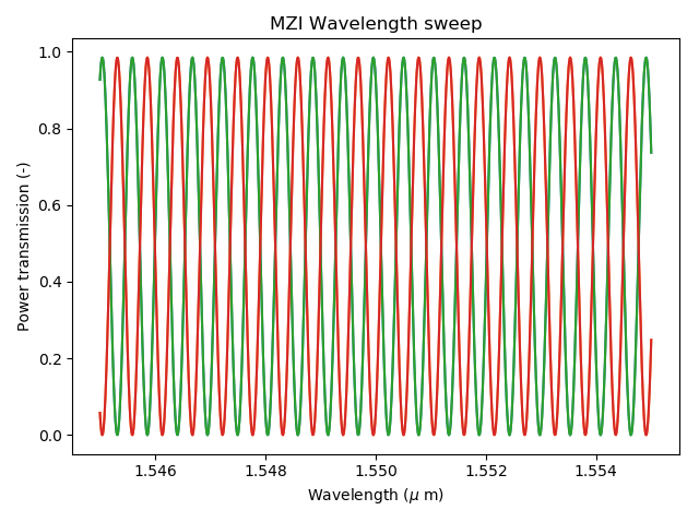
With this in place, you can now run circuit simulations:
import numpy as np
from pylab import plt

mzi_cm = mzi.CircuitModel()

wavelengths = np.linspace(1.545, 1.555, 1001)
S = mzi_cm.get_smatrix(wavelengths=wavelengths)

plt.plot(wavelengths, np.abs(S['out1', 'in1'])**2, label='MZI straight')
plt.plot(wavelengths, np.abs(S['out2', 'in1'])**2, label='MZI cross')
plt.title("MZI Wavelength sweep")
plt.xlabel("Wavelength ($\mu$ m)")
plt.ylabel("Power transmission (-)")
plt.show()
You can also download the full example: demolib_mzi4.py.
Where to go from here
Once you finish this tutorial, you may want to learn more about the following aspects:
If you want to learn more about the concepts of PCells, their views, and parametrization, you can check out: tutorial.
You want to run physical device simulations of basic building blocks: FDTD links.
Adding circuit models to your basic building blocks in order to run circuit simulations: create circuit models
Check out more examples in our sample gallery.